Search results with tag "Slew rate"

MAX3222/MAX3232/MAX3237/MAX3241 - 3.0V to 5.5V, Low …
datasheets.maximintegrated.comslew rate vs. load capacitance (mbaud = vcc) max3222-10 load capacitance (pf) slew rate (v/µs) 500 1000 1500 2000-slew, 1mbps +slew, 1mbps 1 transmitter at full data rate 4 transmitters at 1/16 data rate 3kΩ + cl load each output vcc = 3.3v-slew, 2mbps +slew, 2mbps-7.5-5.0-2.5 0 2.5 5.0 7.5 0 max3237 transmitter output voltage vs. load ...

A CAN Physical Layer Discussion
ww1.microchip.comThe decreased slew rate implies a slower CAN data rate at a given bus length, or a reduced bus length at a given CAN data rate. STANDBY Standby (or sleep) mode is entered by connecting the RS pin to VDD. In sleep mode, the transmitter is switched off and the receiver operates in a reduced power mode. While the receive pin (RXD) is still
ADM483E ±15 kV ESD Protected, Slew Rate …
www.analog.com±15 kV ESD Protected, Slew Rate Limited, 5 V, RS-485 Transceiver ADM483E Rev. A Information furnished by Analog Devices is believed to be accurate and reliable.

MCP2551 High-Speed CAN Transceiver - Microchip Technology
ww1.microchip.comNov 07, 2016 · slope-control resistance value R EXT, a certain slew rate is achieved by applying a specific resistance. Figure 1-1 illustrates typical slew rate values as a function of the slope-control resistance value. 1.4.3 STANDBY MODE The device may be placed in Standby or SLEEP mode by applying a high-level to the R S pin. In SLEEP mode,
NE5534 - Operational Amplifier, Low Noise, Single
www.onsemi.comload, slew rate, low overshoot, etc.). Features • Small-Signal Bandwidth: 10 MHz • Output Drive Capability: 600 , 10 VRMS at VS = 18 V • Input Noise Voltage: 4nV Hz • DC Voltage Gain: 100000 • AC Voltage Gain: 6000 at 10 kHz • Power Bandwidth: 200 kHz • Slew Rate: 13 V/ s • Large Supply Voltage Range: 3.0 to 20 V
NI 6351 Device Specifications - National Instruments
www.ni.comSlew rate 20 V/μs Glitch energy at midscale transition, ±10 V range 10 nV · s External Reference APFI 0 characteristics Input impedance 10 kΩ Coupling DC Protection, device on ±30 V Protection, device off ±15 V Range ±11 V Slew rate 20 V/μs 1 Typical behavior. Time period may be longer due to host system USB performance. Time period
ECEN720: High-Speed Links Circuits and Systems Spring 2021
people.engr.tamu.eduISI is too high and we are sampling too early • If this is negative, then the effective pre-cursor ... (slew rate) Voltage-Mode Summation PI 38 [Joshi VLSI Symp 2009] • For linearity over a wide frequency range, important to control either input or output time constant (slew rate)

MC33272A - Operational Amplifiers, Single Supply, High ...
www.onsemi.comHigh Slew Rate, Low Input Offset Voltage The MC33272/74 series of monolithic operational amplifiers are quality fabricated with innovative Bipolar design concepts. This dual and quad operational amplifier series incorporates Bipolar inputs along with a patented Zip−R−Trim element for input offset voltage reduction.
50 µA, 2 mm × 1.7 mm WLCSP, Low Noise, Heart Rate …
www.analog.comSlew Rate . SR : 0.01 . V/µs . Voltage Noise Density (RTI) e. n . f = 1 kHz : 120 . nV/√Hz . Peak-to-Peak Voltage Noise (RTI) e n p-p : f = 0.1 Hz to 10 Hz . 7 . µV p-p . f = 0.5 Hz to 40 Hz . 9 . µV p-p . RIGHT LEG DRIVE AMPLIFIER (A2) Quiescent Supply Current . 7.5 . 10 . µA : Output Swing . R. L = 50 kΩ . 0.1 +V S − 0.1 . V . Short ...

AD8065/AD8066 (Rev. L) - Analog Devices
www.analog.comthey offer a high slew rate of 180 V/µs, excellent distortion (SFDR of −88 dBc @ 1 MHz), extremely high common-mode rejection of −100 dB, and a low input offset voltage of 1.5 mV maximum under warmed up conditions. The AD8065/AD8066 operate using only a 6.4 mA/amplifier typical supply current and are
LTC2057/LTC2057HV - High Voltage, Low Noise Zero-Drift ...
www.analog.comand a 0.45V/μs (typ) slew rate. Wide supply range, combined with low noise, low offset, and excellent PSRR and CMRR make the LTC2057 and LTC2057HV well suited for high dynamic-range test, measurement, and instrumentation systems. L, LT, LTC, LTM, Linear Technology, Over-The-Top, and the Linear logo are registered
LM321A/ LM358A/ LM324A
3peakic.com.cnSR Slew Rate G = 1, 2V step 0.5 V/μs t S Settling Time, 0.1% G = 1, 2V step 4 μs Settling Time, 0.01% 5 μs PM Phase Margin V S = 30V, R L =1K, C L =100pF 60 ° GM Gain Margin V S = 30V, R L =1K, C L =100pF 15 dB Channel Separation f = 1 kHz to 20 kHz 120 dB Noise Performance E N

MAX13487E/MAX13488E Half-Duplex RS-485-/RS-422- …
datasheets.maximintegrated.comThe MAX13488E driver slew rate is not limited, allowing transmit speeds up to 16Mbps. The MAX13487E/MAX13488E feature a 1/4-unit load receiver input impedance, allowing up to 128 trans-ceivers on the bus. These devices are intended for half-duplex communications. All driver outputs are protected to ±15kV ESD using the Human Body Model.

Operational Amplifier Circuits - MIT OpenCourseWare
ocw.mit.edureactive elements. Providing we keep the operating conditions out of the slew rate limit then this is a reasonable model. Here we wish to extend this picture of op amp operation to include circuits that are designed to be frequency dependent. This will enable the construction of active filters, integrators, differentiators and oscillators.
LTC7004 (Rev. C)
www.analog.comHigh Voltage, High Side Switch with 100% Duty Cycle n Wide Operating VIN: Up to 60V n 1Ω Pull-Down, 2.2Ω Pull-Up for Fast Turn-On and Turn-Off Times with 35ns Propagation Delays n Internal Charge Pump for 100% Duty Cycle n Adjustable Turn-On Slew Rate n Gate Driver Supply from 3.5V to 15V n Adjustable VIN Overvoltage Lockout
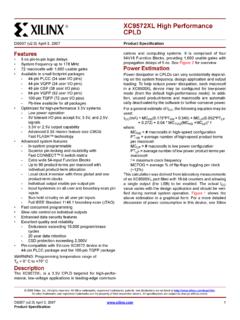
0 R XC9572XL High Performance CPLD - Xilinx
www.xilinx.com• Slew rate control on individual outputs • Enhanced data security features • Excellent quality and reliability - Endurance exceeding 10,000 program/erase cycles - 20 year data retention - ESD protection exceeding 2,000V • Pin-compatible with 5V-core XC9572 device in the 44-pin PLCC package and the 100-pin TQFP package

R XC2C32A CoolRunner-II CPLD - Xilinx
www.xilinx.comconfigurations include slew rate limit, bus hold, pull-up, open drain, and programmable grounds. A Schmitt trigger input is available on a per input pin basis. In addition to stor-ing macrocell output states, the macrocell registers can be configured as "direct input" registers to …

LT1010 - Fast ±150mA Power Buffer - Analog Devices
www.analog.comSlew Rate VS = ±15V, VIN = ±10V, VOUT = ±8V, RL = 100Ω 75 V/µs VSOS + Positive Saturation Offset IOUT = 0 (Note 5) l 1.0 1.1 V V VSOS – Negative Saturation Offset IOUT = 0 (Note 5) l 0.2 0.3 V V RSAT Saturation Resistance IOUT = ±150mA (Note 5) l 22 28 Ω Ω VBIAS Bias Terminal Voltage RBIAS = 20Ω (Note 6) l 700 560 840 880 mV mV IS ...
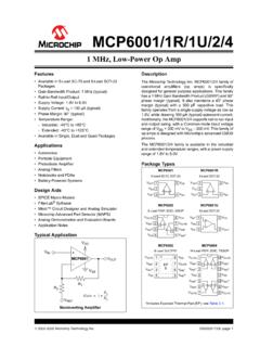
MCP6001/1R/1U/2/4 - 1 MHz, Low-Power Op Amp
ww1.microchip.comMay 14, 2019 · Slew Rate SR — 0.6 — V/µs Noise Input Noise Voltage Eni — 6.1 — µVp-p f = 0.1 Hz to 10 Hz ... Note: The graphs and tables provided following this note are a statistical summary based on a limited number of samples and are provided for informational purposes only. The performance characteristics listed herein
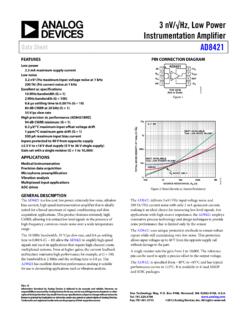
3 nV/√Hz, Low Power Instrumentation Amplifier Data Sheet ...
www.analog.com35 V/µs slew rate . High precision dc performance (AD8421BRZ) 94 dB CMRR minimum (G = 1) 0.2 µV/°C maximum input offset voltage drift . 1 ppm/°C maximum gain drift (G = 1) 500 pA maximum input bias current . Inputs protected TOTAL NOISE DENSITY AT 1kHz (V/√Hz)to 40 V from opposite supply . ±2.5 V to ±18 V dual supply (5 V to 36 V single ...

a Low Noise, Precision, High Speed Operational Amplifier ...
www.analog.comDec 20, 1980 · High Speed, 17 V/ s Slew Rate 63 MHz Gain Bandwidth Low Input Offset Voltage, 10 V Excellent CMRR, 126 dB (Common-Voltage @ 11 V) High Open-Loop Gain, 1.8 Million Replaces 725, OP-07, SE5534 In Gains > 5 Available in Die Form GENERAL DESCRIPTION The OP37 provides the same high performance as the OP27,
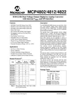
MCP4802/4812/4822 Data Sheet - Microchip Technology
ww1.microchip.comSlew Rate SR — 0.55 — V/µs Short Circuit Current ISC —15 24 mA Settling Time t SETTLING — 4.5 — µs Within 1/2 LSb of final value from 1/4 to 3/4 full-scale range Dynamic Performance (Note 2) DAC-to-DAC Crosstalk — <10 — nV-s Major Code Transition Glitch — 45 — nV-s 1 LSb change around major carry

AD797 (Rev. K) - Analog Devices
www.analog.comSlew Rate R LOAD Settling Time to 0.0015% 10 V step ±15 V 800 1200 800 1200 ns COMMON-MODE REJECTION V CM = CMVR ±5 V, ±15 V 114 130 120 130 dB T MIN to T MAX 110 120 ... current should be limited to less than 25 mA by series protection resistors. Note, however, that this degrades the low noise performance of the device. ...

Iron and Steel - USGS
pubs.usgs.govThe U.S. iron and steel industry produced raw steel in 2020 with an estimated value of about $91 billion, an 12% decrease from $104 billion in 2019 and $103 billion in 2018. Pig iron and raw steel was produced by three companies operating integrated steel mills in 11 locations. Raw steel was produced by 51 companies at 98 minimills.
Similar queries
Slew Rate, Slew, Rate, A CAN Physical Layer Discussion, ESD Protected, Slew Rate, ESD Protected, Slew Rate Limited, 5, Analog Devices, High, Limited, Protected, MIT OpenCourseWare, Switch, XC9572XL, Xilinx, XC2C32A, MCP6001/1R/1U/2/4, 1 MHz, Low-Power Op Amp, OP37, Iron and steel, Raw steel, And raw steel, Steel