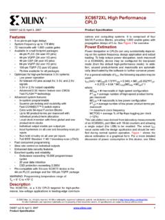
Transcription of R XC2C32A CoolRunner-II CPLD - Xilinx
1 DS310 ( ) November 6, Specification 2004 2008 Xilinx , Inc. All Xilinx trademarks, registered trademarks, patents, and disclaimers are as listed at All other trademarks and registered trademarks are the property of their respective owners. All specifications are subject to change without Optimized for systems-As fast as ns pin-to-pin logic delays-As low as 12 A quiescent current Industry s best micron CMOS CPLD-Optimized architecture for effective logic synthesis-Multi-voltage I/O operation: through Available in multiple package options-32-land QFN with 21 user I/Os-44-pin VQFP with 33 user I/Os-56-ball CP BGA with 33 user I/Os-Pb-free available for all packages Advanced system features-Fastest in system programming ISP using IEEE 1532 (JTAG) JTAG Boundary Scan Test-Optional Schmitt-trigger input (per pin)-Two separate I/O banks-RealDigital 100% CMOS product term generation-Flexible clocking modes-Optional DualEDGE triggered registers-Global signal options with macrocell control Multiple global clocks with phase selection per macrocell Multiple global output enables Global set/reset-Efficient control term clocks, output enables and set/resets for each macrocell and shared across function blocks-Advanced design security-Open-drain output option for Wired-OR and LED drive-Optional configurable grounds on unused I/Os-Optional bus-hold, 3-state, or weak pullup on selected I/O pins-Mixed I/O voltages compatible with.
2 And logic levels-PLA architecture Superior pinout retention 100% product term routability across function block-Hot pluggableRefer to the CoolRunner -II family data sheet for the archi-tecture CoolRunner -II 32-macrocell device is designed forboth high performance and low power applications. Thislends power savings to high-end communication equipmentand high speed to battery operated devices. Due to the lowpower stand-by and dynamic operation, overall system reli-ability is device consists of two Function Blocks interconnectedby a low power Advanced Interconnect Matrix (AIM). TheAIM feeds 40 true and complement inputs to each FunctionBlock. The Function Blocks consist of a 40 by 56 P-termPLA and 16 macrocells which contain numerous configura-tion bits that allow for combinational or registered modes ofoperation. Additionally, these registers can be globally reset or presetand configured as a D or T flip-flop or as a D latch.
3 Thereare also multiple clock signals, both global and local productterm types, configured on a per macrocell basis. Output pinconfigurations include slew rate limit, bus hold, pull-up,open drain, and programmable grounds. A Schmitt triggerinput is available on a per input pin basis. In addition to stor-ing macrocell output states, the macrocell registers can beconfigured as "direct input" registers to store signals directlyfrom input pins. Clocking is available on a global or Function Block global clocks are available for all Function Blocks as asynchronous clock source. Macrocell registers can be indi-vidually configured to power up to the zero or one state. Aglobal set/reset control line is also available to asynchro-nously set or reset selected registers during local clock, synchronous clock-enable, asynchro-nous set/reset, and output enable signals can be formedusing product terms on a per-macrocell or per-FunctionBlock basis.
4 The CoolRunner-II 32-macrocell CPLD is I/O compatiblewith standard LVTTL and LVCMOS18, LVCMOS25, andLVCMOS33 (see Ta b l e 1). This device is also I/O com-patible with the use of Schmitt-trigger feature that eases voltage translation is I/O bank-ing. Two I/O banks are available on the CoolRunner-II 32 Amacrocell device that permit easy interfacing to , , , and CoolRunner-II CPLDDS310 ( ) November 6, 200800 Product SpecificationRXC2C32A CoolRunner-II ( ) November 6, 2008 Product SpecificationRRealDigital Design TechnologyXilinx CoolRunner-II CPLDs are fabricated on micron process technology which is derived from lead-ing edge FPGA product development. CoolRunner-IICPLDs employ RealDigital, a design technique that makesuse of CMOS technology in both the fabrication and designmethodology. RealDigital design technology employs a cas-cade of CMOS gates to implement sum of products insteadof traditional sense amplifier methodology.
5 Due to this tech-nology, Xilinx CoolRunner-II CPLDs achieve both high per-formance and low power operation. Supported I/O StandardsThe CoolRunner-II CPLD 32 macrocell features bothLVCMOS and LVTTL I/O implementations. See Ta b l e 1 forI/O standard voltages. The LVTTL I/O standard is a generalpurpose EIA/JEDEC standard for applications that usean LVTTL input buffer and Push-Pull output buffer. TheLVCMOS standard is used in , , and applica-tions. CoolRunner-II CPLDs are also I/O compatiblewith the use of Schmitt-trigger inputs. Ta b l e 1 : I/O Standards for XC2C32 AIOSTANDARD AttributeOutput VCCIOI nput VCCIOI nput VREFB oard Termination Vol tag e C M O S 1 5(1) requires Schmitt-trigger 1: ICC vs. FrequencyTa b l e 2 : ICC vs. Frequency (LVCMOS TA = 25 C)(1)Frequency (MHz)0255075100150175200225250300 Typical ICC (mA) : up/down, resettable binary counter (one counter per function block).
6 Frequency (MHz)DS091_01_030105 ICC (mA)00510152030025020015010050XC2C32A CoolRunner-II CPLDDS310 ( ) November 6, SpecificationRRecommended Operating ConditionsDC Electrical Characteristics Over Recommended Operating Conditions Absolute Maximum RatingsSymbolDescriptionValueUnitsVCCS upply voltage relative to ground to voltage for output drivers to (2)JTAG input voltage limits to input supply voltage to (1)Input voltage relative to ground to (1)Voltage applied to 3-state output to (3)Storage Temperature (ambient) 65 to +150 CTJJ unction Temperature+150 CNotes: DC undershoot below GND must be limited to either or 10 mA, whichever is easiest to achieve. During transitions, the device pins might undershoot to or overshoot to + , provided this overshoot or undershoot lasts less than 10 ns and with the forcing current being limited to 200 over commercial temperature soldering guidelines and thermal considerations, see the Device Packaging information on the Xilinx website.
7 For Pb free packages, see voltage for internal logic and input buffersCommercial TA = 0 C to +70 TA = 40 C to +85 voltage for output drivers @ voltage for output drivers @ voltage for output drivers @ voltage for output drivers @ programming current CommercialVCC = , VCCIO = AICCSBS tandby current IndustrialVCC = , VCCIO = AICC(1)Dynamic current f = 1 = 50 input capacitancef = 1 MHz-10pFCCLKG lobal clock input capacitancef = 1 MHz-12pFCIOI/O capacitancef = 1 MHz-10pFIIL(2)Input leakage currentVIN = 0V or VCCIO to +/-1 AIIH(2)I/O High-Z leakageVIN = 0V or VCCIO to +/-1 ANotes: up/down resettable binary counter (one per Function Block) tested at VCC = VCCIO = Quality and Reliability section of the CoolRunner-II family data CoolRunner-II ( ) November 6, 2008 Product SpecificationRLVCMOS and LVTTL DC Voltage SpecificationsLVCMOS DC Voltage SpecificationsLVCMOS DC Voltage SpecificationsLV C M O S DC Voltage SpecificationsSymbolParameterTest source level input level input voltage level output voltageIOH = 8 mA, VCCIO = 3 VVCCIO = mA, VCCIO = 3 VVCCIO level output voltageIOL = 8 mA, VCCIO = = mA, VCCIO = source level input + (1)VVILLow level input voltage level output voltageIOH = 8 mA, VCCIO = = mA, VCCIO = level output voltageIOL = 8 mA, VCCIO = = , VCCIO = VIH Max value represents the JEDEC specification for LVCMOS25.
8 The CoolRunner-II CPLD input buffer can tolerate up to without physical (1)Test source level input x VCCIOVCCIO + (1)VVILLow level input voltage x VCCIOVVOHHigh level output voltageIOH = 8 mA, VCCIO = = mA, VCCIO = level output voltageIOL = 8 mA, VCCIO = = mA, VCCIO = VIH Max value represents the JEDEC specification for LVCMOS18. The CoolRunner-II CPLD input buffer can tolerate up to without physical source +Input hysteresis threshold x x VCCIOVVT- x x VCCIOVVOHHigh level output voltageIOH = 8 mA, VCCIO = = mA, VCCIO = level output voltageIOL = 8 mA, VCCIO = = mA, VCCIO = : used on CoolRunner-II CPLDDS310 ( ) November 6, SpecificationRSchmitt Trigger Input DC Voltage SpecificationsAC Electrical Characteristics Over Recommended Operating Conditions SymbolParameterTest source +Input hysteresis threshold x x VCCIOVVT- x x delay single delay OR input register clock setup time fast (single p-term) time (OR array) input register hold hold to (1)Internal toggle rate-500-300 MHzFSYSTEM1(2)Maximum system frequency-323-200 MHzFSYSTEM2(2)Maximum system frequency-303-182 MHzFEXT1(3)Maximum external frequency-179-137 MHzFEXT2(3)Maximum external frequency-172-128 MHzTPSUDD irect input register p-term clock setup clock setup time (single p-term) clock setup time (OR array)
9 Input register p-term clock hold clock clock to Global OE to output OE to output driven OE to output OP-term set/reset to output set/reset to output clock enable setup clock enable hold clock pulse width High or pulse width High or preset/reset pulse width (High or Low) (4)Configuration time-50-50 sNotes: is the maximum clock frequency to which a T-Flip Flop can reliably toggle (see the CoolRunner-II family data sheet). (1/TCYCLE) is the internal operating frequency for a device fully populated with one 16-bit counter through one p-term per macrocell while FSYSTEM2 is through the OR (1/TSU1+TCO) is the maximum external frequency using one p-term while FEXT2 is through the OR configuration current during TCONFIG is 500 CoolRunner-II ( ) November 6, 2008 Product SpecificationRInternal Timing ParametersSymbolParameter(1) DelaysTINI nput buffer register input Clock buffer set/reset buffer 3-state buffer buffer buffer enable/disable DelaysTCTC ontrol term p-term delay p-term delay DelayTPDII nput to output before clock (transparent latch)
10 Before clock after Enable clock setup time Enable clock hold time to output to output DelaysTFFeedback to global OE Standard Time Adder Delays CMOSTHYS15 Hysteresis input slew rate Standard Time Adder Delays CMOSTHYS18 Hysteresis input slew rate CoolRunner-II CPLDDS310 ( ) November 6, SpecificationRSwitching CharacteristicsAC Test CircuitI/O Standard Time Adder Delays CMOSTIN25 Standard input input slew rate Standard Time Adder Delays CMOS/TTLTIN33 Standard input input slew rate : ns input pin signal Timing Parameters (Continued)SymbolParameter(1) 2: Derating Curve for TPD Number of Outputs Switching124 8 = VCCIO = @ 25oCTPD2 (ns) 3: AC Load CircuitR1 VCCCLR2 Device Under TestOutput TypeLVTTL33 LVCMOS33 LVCMOS25 LVCMOS18 LVCMOS15CL includes test fixtures and probe capacitance. nsec maximum rise/fall times on 275 188 150 R2235 275 188 150 CL35 pF35 pF35pF35pF35pFDS310_03_102108 Test PointXC2C32A CoolRunner-II ( ) November 6, 2008 Product SpecificationRTypical I/O Output CurvesFigure 4.