Transcription of IRF1407 - Infineon Technologies
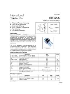
1 @ TC = 25 CContinuous Drain Current, VGS @ 10V130 ID @ TC = 100 CContinuous Drain Current, VGS @ 10V92 AIDMP ulsed Drain Current 520PD @TC = 25 CPower Dissipation330 WLinear Derating CVGSGate-to-Source Voltage 20 VEASS ingle Pulse Avalanche Energy 390mJIARA valanche Current See , 12b, 15, 16 AEARR epetitive Avalanche Energy mJdv/dtPeak Diode Recovery dv/dt Junction and-55 to + 175 TSTGS torage Temperature RangeSoldering Temperature, for 10 seconds300 ( from case ) CMounting Torque, 6-32 or M3 screw10 lbf in ( m)HEXFET Power MOSFETS pecifically designed for Automotive applications, this Stripe Planardesign of HEXFET Power MOSFETs utilizes the lastest processingtechniques to achieve extremely low on-resistance per silicon features of this HEXFET power MOSFET are a 175 C junctionoperating temperature, fast switching speed and improved repetitiveavalanche rating.
2 These benefits combine to make this design an extremelyefficient and reliable device for use in Automotive applications and a widevariety of other Maximum RatingsVDSS = 75 VRDS(on) = ID = 130A Description10/11 Advanced Process Technology Ultra Low On-Resistance Dynamic dv/dt Rating 175 C Operating Temperature Fast Switching Repetitive Avalanche Allowed up to TjmaxBenefitsTypical Applications Integrated Starter Alternator 42 Volts Automotive Electrical SystemsAUTOMOTIVE MOSFETTO-220 ABPD - JCJunction-to-Case CSCase-to-Sink, Flat, Greased C/WR JAJunction-to-Ambient 62 Thermal Typ. Max. Units ConditionsV(BR)DSSD rain-to-Source Breakdown Voltage75 VVGS = 0V, ID = 250 A V(BR)DSS/ TJBreakdown Voltage Temp.
3 Coefficient V/ C Reference to 25 C, ID = 1mARDS(on)Static Drain-to-Source On-Resistance VGS = 10V, ID = 78A VGS(th)Gate Threshold = 10V, ID = 250 AgfsForward Transconductance74 SVDS = 25V, ID = 78A 20 AVDS = 75V, VGS = 0V 250 VDS = 60V, VGS = 0V, TJ = 150 CGate-to-Source Forward Leakage 200 VGS = 20 VGate-to-Source Reverse Leakage -200nAVGS = -20 VQgTotal Gate Charge 160250ID = 78 AQgsGate-to-Source Charge 3552nCVDS = 60 VQgdGate-to-Drain ("Miller") Charge 5481 VGS = 10V td(on)Turn-On Delay Time 11 VDD = 38 VtrRise Time 150 ID = 78 Atd(off)Turn-Off Delay Time 150 RG = tfFall Time 140 VGS = 10V Between lead, 6mm ( )from packageand center of die contactCissInput Capacitance 5600 VGS = 0 VCossOutput Capacitance 890 pFVDS = 25 VCrssReverse Transfer Capacitance 190 = , See Fig.
4 5 CossOutput Capacitance 5800 VGS = 0V, VDS = , = Capacitance 560 VGS = 0V, VDS = 60V, = Output Capacitance 1100 VGS = 0V, VDS = 0V to 60 VnHElectrical Characteristics @ TJ = 25 C (unless otherwise specified)LDInternal Drain InductanceLSInternal Source Inductance Leakage CurrentSDG ParameterMin. Units ConditionsISContinuous Source CurrentMOSFET symbol(Body Diode) showing theISMP ulsed Source Currentintegral reverse(Body Diode) p-n junction Forward Voltage = 25 C, IS = 78A, VGS = 0V trrReverse Recovery Time 110170nsTJ = 25 C, IF = 78 AQrrReverse RecoveryCharge 390590nCdi/dt = 100A/ s tonForward Turn-On TimeIntrinsic turn-on time is negligible (turn-on is dominated by LS+LD)Source-Drain Ratings and Characteristics130 520A Repetitive rating; pulse width limited by max.
5 Junction temperature. (See fig. 11). Starting TJ = 25 C, L = RG = 25 , IAS = 78A. (See Figure 12). ISD 78A, di/dt 320A/ s, VDD V(BR)DSS, TJ 175 C Pulse width 400 s; duty cycle 2%.Notes: Coss eff. is a fixed capacitance that gives the same charging time as Coss while VDS is rising from 0 to 80% VDSS . Calculated continuous current based on maximum allowable junction temperature. Package limitation current is 75A. Limited by TJmax , see , 12b, 15, 16 for typical repetitive avalanche 4. Normalized On-Resistancevs. TemperatureFig 2. Typical Output CharacteristicsFig 1. Typical Output CharacteristicsFig 3. Typical Transfer , Drain-to-Source Voltage (V)1101001000ID, Drain-to-Source Current (A) s PULSE WIDTHTj = 25 C VGSTOP 15V 10V , Drain-to-Source Voltage (V)1101001000ID, Drain-to-Source Current (A) s PULSE WIDTHTj = 175 C VGSTOP 15V 10V , Gate-to-Source Voltage (V) , Drain-to-Source Current ( )TJ = 25 CTJ = 175 CVDS = 15V20 s PULSE , Junction Temperature( C)
6 R , Drain-to-Source On Resistance(Normalized)JDS(on) V=I= 8. Maximum Safe Operating AreaFig 6. Typical Gate Charge VoltageFig 5. Typical Capacitance VoltageFig 7. Typical Source-Drain DiodeForward Voltage110100 VDS, Drain-to-Source Voltage (V)100100010000100000C, Capacitance(pF)CossCrssCissVGS = 0V, f = 1 MHZCiss = Cgs + Cgd, Cds SHORTEDCrss = Cgd Coss = Cds + Cgd0408012016020003691215Q , Total Gate Charge (nC)V , Gate-to-Source Voltage (V)GGS I=D78A V= 15 VDSV= 37 VDSV= , Source-toDrain Voltage (V) , Reverse Drain Current (A)TJ = 25 CTJ = 175 CVGS = 0V1101001000 VDS , Drain-toSource Voltage (V)110100100010000ID, Drain-to-Source Current (A)Tc = 25 CTj = 175 CSingle Pulse1msec10msecOPERATION IN THIS AREA LIMITED BY RDS(on)100 9.
7 Maximum Drain Current TemperatureVDS90%10%VGStd(on)trtd(off)tf VDSP ulse Width 1 sDuty Factor % +-VDDFig 10a. Switching Time Test CircuitFig 10b. Switching Time WaveformsFig 11. Maximum Effective Transient Thermal Impedance, Junction-to-Case255075100125150175020406 080100120140T , Case Temperature( C)I , Drain Current (A) CD LIMITED BY 1 Notes:1. Duty factor D =t / t2. Peak T=Px Z+ T12 JDMthJCC PttDM12t , Rectangular Pulse Duration (sec)Thermal Response(Z ) = SINGLE PULSE(THERMAL RESPONSE) F50K .2 F12 VCurrent RegulatorSame Type as Sampling Resistors+-10 VFig 13b. Gate Charge Test CircuitFig 13a. Basic Gate Charge WaveformFig 12c.
8 Maximum Avalanche Energyvs. Drain CurrentFig 12b. Unclamped Inductive WaveformsFig 12a. Unclamped Inductive Test CircuittpV(BR) +-VDDDRIVERA15V20 VFig 14. Threshold Voltage vs. Temperature25507510012515017501302603905 20650 Starting T , Junction Temperature( C)E , Single Pulse Avalanche Energy (mJ)JAS IDTOPBOTTOM32A 55A 78A -75-50-250255075100125150175200TJ , Temperature ( C ) (th) Gate threshold Voltage (V)ID = 250 15. Typical Avalanche Current 16. Maximum Avalanche Energyvs. TemperatureNotes on Repetitive Avalanche Curves , Figures 15, 16:(For further info, see AN-1005 at )1. Avalanche failures assumption: Purely a thermal phenomenon and failure occurs at a temperature far in excess of Tjmax.
9 This is validated for every part Safe operation in Avalanche is allowed as long asTjmax is not Equation below based on circuit and waveforms shown in Figures 12a, PD (ave) = Average power dissipation per single avalanche BV = Rated breakdown voltage ( factor accounts for voltage increase during avalanche).6. Iav = Allowable avalanche T = Allowable rise in junction temperature, not to exceed Tjmax (assumed as 25 C in Figure 15, 16). tav = Average time in avalanche. D = Duty cycle in avalanche = tav f ZthJC(D, tav) = Transient thermal resistance, see figure 11)PD (ave) = 1/2 ( BV Iav) = T/ ZthJCIav = 2 T/ [ BV Zth]EAS (AR) = PD (ave) (sec)1101001000 Avalanche Current (A) Cycle = Single avalanche Current vs avalanche pulsewidth, tav assuming Tj = 25 C due to avalanche TJ , Junction Temperature ( C)0100200300400 EAR , Avalanche Energy (mJ)
10 TOP Single Pulse BOTTOM 10% Duty CycleID = Diode Recovery dv/dt Test Recoverydv/dtRipple 5%Body Diode Forward DropRe-AppliedVoltageReverseRecoveryCurr entBody Diode ForwardCurrentVGS=10 VVDDISDD river Gate VDSW aveformInductor CurentD = P. W .Period+-+++--- RGVDD dv/dt controlled by RG ISD controlled by Duty Factor "D" - Device Under *Circuit Layout Considerations Low Stray Inductance Ground Plane Low Leakage Inductance Current Transformer * Reverse Polarity of for P-ChannelVGS[ ][ ]** VGS = for Logic Level and 3V Drive Devices[ ] **Fig 17. For N-channel HEXFET power ASSIGNMENTS 1 - G A T E 2 - D R A IN 3 - S O U R C E 4 - D R A IN- B (.)



![CS12N65F+A9H[1] - crhj.com.cn](/cache/preview/8/6/0/a/d/0/b/6/thumb-860ad0b6af153a32a350278788bfd392.jpg)