Transcription of Lecture 6 Scanning Tunneling Microscopy (STM) • …
1 Lecture 6 Scanning Tunneling Microscopy (STM) General components of STM; Tunneling current; Feedback system; Tip --- the probe. Brief Overview of STM Inventors of STM Nobel Laureates Heinrich Rohrer and Gerd Binnig The Nobel Prize in Physics 1986 Brief History of STM The first member of SPM family, Scanning Tunneling Microscopy (STM), was developed In 1982, by Gerd Binnig and Heinrich Rohrer at IBM in Zurich created the ideas of STM (Phys. Rev. Lett., 1982, vol 49, p57). Both of the two people won 1986 Nobel prize in physics for their brilliant invention.
2 Nobel Laureates Heinrich Rohrer and Gerd Binnig (B. 1947) STM is really small in size. Basic components of STM: Five basic components: tip, scanner, amplifier (nA), (bias), loop (current). Tunneling current from tip to sample or vice-versa depending on bias; Current is exponentially dependent on distance; Raster Scanning gives 2D image; Feedback is normally based on constant current, thus measuring the height on surface. The scanner can be mounted with the tip or the sample stage. STM Tips STM tip should be conducting (metals, like Pt); STM plays with the very top (outermost) atom at the tip and the nearest atom on sample; so the whole tip is not necessarily very sharp in shape, different from the case of AFM, where spatial contact is necessary and crucial for feedback.
3 How do we obtain these wonderful Tunneling tips where only one atom is at the top? Answer: really easy to obtain such tips, simply by cutting a thin metal wire using a wire cutter --- there is always a single atom left over at the very top. Tunneling Current a result of the overlap of tip and sample electron wavefunctions In a metal, the energy levels of the electrons are filled up to a particular energy, known as the Fermi energy EF. In order for an electron to leave the metal, it needs an additional amount of energy , the so-called work function.
4 When the specimen and the tip are brought close to each other, there is only a narrow region of empty space left between them. On either side, the electrons are present up to the Fermi energy. They need to overcome a barrier to travel from tip to specimen or vice versa. If the distance d between specimen and tip is small enough, electrons can tunnel through the vacuum barrier. When a voltage V is applied between specimen and tip, the Tunneling effect results in a net electron current. In this example from specimen to tip. This is the Tunneling current.
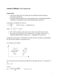
5 Two requirements: 1. small distance --- electron wavefunction overlap 2. bias --- for net current flow. Electron density of states: Fermi level Electron density of states: Fermi level The electrons fill up the energy valley in the sample until there are no more electrons. The top energy level at which electrons sit is called the Fermi level, F. For every energy , the density of states is the number of electrons sitting within of , divided by . So, for the energy shown above as a blue strip, DOS( ) is approximately 7 /.
6 Tip and Sample: lined up exactly under zero bias The electrons in the tip and the sample are sitting in two separate valleys, separated by a hill which is the vacuum barrier. Electron density of states: Fermi level Electrons are happy sitting in either the tip or the sample, they're sitting in nice energy valleys. It takes energy to remove an electron into free space. We can think of the vacuum around the tip as an energy hill that the electron would need to climb in order to escape. The height of this energy hill is called the work function.
7 In order to bring an electron up and over the vacuum energy barrier from the tip into the sample (or vice versa), we would need to supply a very large amount of energy. Climbing hills is hard work! Luckily for us, quantum mechanics tells us that the electron can tunnel right through the barrier. Note: this only works for particles (with both wave and particle characteristics), not for macroscopic objects. Don't you try walking through any closed doors! As long as both the tip and the sample are held at the same electrical potential, their Fermi levels line up exactly.
8 There are no empty states on either side available for Tunneling into! This is why we apply a bias voltage between the tip and the sample. Tunneling current at bias By applying a bias voltage to the sample with respect to the tip, we effectively raise the Fermi level of the sample with respect to the tip. Now we have empty states available for Tunneling into. Tunneling Current A thin metal tip is brought in close proximity of the sample surface. At a distance of only a few , the overlap of tip and sample electron wavefunctions is large enough for an electron Tunneling to occur.
9 When an electrical voltage V is applied between sample and tip, this Tunneling phenomenon results in a net electrical current, the Tunneling current . This current depends on the tip-surface distance d, on the voltage V, and on the height of the barrier : This (approximate) equation shows that the Tunneling current obeys Ohm s law, the current I is proportional to the voltage V. The current depends exponentially on the distance d. For a typical value of the work function of 4 eV for a metal, the Tunneling current reduces by a factor 10 for every nm increase in d.
10 This means that over a typical atomic diameter of nm, the Tunneling current changes by a factor 1000! This is what makes the STM so sensitive. The Tunneling current depends so strongly on the distance that it is dominated by the contribution flowing between the last atom of the tip and the nearest atom in the specimen --- single-atom imaging! : the work function (energy barrier), e: the electron charge, m: the electron mass, h: the Planck s constant, V: applied voltage, d: tip-sample distance. Next page: of common metals. Work Function of Common Metals Metal (eV) (Work Function) Ag (silver) Al (aluminum) Au (gold) Cs (cesium) Cu (copper) Li (lithium) Pb (lead) Sn (tin) Chromium Molybdenum Stainless Steel Gold Tungsten Copper Nickel Basic components of STM: Five basic components: tip, scanner, amplifier (nA), (bias), loop (current).