Transcription of LM1596/LM1496 Balanced Modulator …
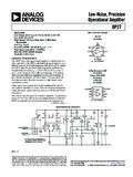
1 TL/H/7887LM1596/ lm1496 Balanced Modulator -DemodulatorFebruary 1995LM1596/ lm1496 Balanced Modulator -DemodulatorGeneral DescriptionThe LM1596/LM1496 are doubled Balanced Modulator -de-modulators which produce an output voltage proportional tothe product of an input (signal) voltage and a switching (car-rier) signal. Typical applications include suppressed carriermodulation, amplitude modulation, synchronous detection,FM or PM detection, broadband frequency doubling lm1596 is specified for operation over theb55 Ctoa125 C military temperature range. The lm1496 is speci-fied for operation over the 0 Ctoa70 C temperature carrier suppression65 dB typical at MHz50 dB typical at 10 MHzYAdjustable gain and signal handlingYFully Balanced inputs and outputsYLow offset and driftYWide frequency response up to 100 MHzSchematic and Connection DiagramsTL/H/7887 1 Numbers in parentheses show DIP Can PackageTL/H/7887 2 Top ViewNote:Pin 10 is connected electrically to thecase through the device Number LM1496H or lm1596 HSee NS Package Number H08 CDual-In-Line and Small Outline PackagesTL/H/7887 3 Order Number LM1496M or lm1496 NSee NS Package Number M14A or N14AC1995 National Semiconductor CorporationRRD-B30M115/Printed in U.
2 S. Maximum RatingsIf Military/Aerospace specified devices are required,please contact the National Semiconductor SalesOffice/Distributors for availability and Power Dissipation (Note 1)500 mWApplied Voltage (Note 2)30 VDifferential Input Signal (V7bV8) Input Signal (V4bV1)g(5aI5R0)VInput Signal (V2bV1,V3bV4) Current (I5)12mAOperating Temperature Range LM1596b55 Ctoa125 CLM14960 Ctoa70 CStorage Temperature Rangeb65 Ctoa150 CSoldering Information#Dual-In-Line PackageSoldering (10 seconds)260 C#Small Outline PackageVapor Phase (60 seconds)215 CInfrared (15 seconds)220 CSee AN-450 Surface Mounting Methods and their effectson Product Reliability for other methods of soldering sur-face mount Characteristics(TAe25 C, unless otherwise specified, see test circuit)ParameterConditionsLM1596LM1496 UnitsMin Typ Max Min Typ MaxCarrier FeedthroughVCe60 mVrms sine kHz, offset adjustedVCe60 mVrms sine wave140140mVrmsfCe10 kHz, offset adjustedVCe300 mVppsquare kHz, offset adjustedVCe300 mVppsquare wave20 10020 150 kHz, not offset adjustedCarrier SuppressionfSe10 kHz, 300 mVrms50 6550 65dBfCe500 kHz, 60 mVrms sine wave offset adjustedfSe10 kHz, 300 mVrms5050dBfCe10 MHz, 60 mVrms sine wave offset adjustedTransadmittance BandwidthRLe50X300300 MHzCarrier Input Port, VCe60 mVrms sine kHz, 300 mVrms sine waveSignal Input Port, VSe300 mVrms sine Gain, Signal ChannelVSe100 mVrms, VdcInput Resistance, Signal VdcInput Capacitance, Signal Port VdcSingle Ended Output Resistance fe10 MHz4040kXSingle Ended Outputfe10 Bias Current(I1aI4)
3 /212 2512 30mAInput Bias Current(I7aI8)/212 2512 30mAInput Offset Current(I1bI4) Offset Current(I7bI8) Temperature(b55 CkTAka125 C) CCoefficient of Input(0 CkTAka70 C) COffset CurrentOutput Offset Current(I6bI9)14501460mAAverage Temperature(b55 CkTAka125 C)90nA/ CCoefficient of Output(0 CkTAka70 C)90nA/ COffset Current2 Electrical Characteristics(TAe25 C, unless otherwise specified, see test circuit) (Continued)ParameterConditionsLM1596LM14 96 UnitsMinTypMaxMinTypMaxSignal Port Common Voltage RangeSignal Port Common Vdcb85b85dBRejection RatioCommon Mode VoltageDifferential Output Supply Current(I6aIg) Supply Current(I10) Dissipation3333mWNote 1: lm1596 rating applies to case temperatures toa125 C; derate linearly at mW/ C for ambient temperature above 75 C. lm1496 rating applies to casetemperatures toa70 2:Voltage applied between pins 6-7, 8-1, 9-7, 9-8, 7-4, 7-1, 8-4, 6-8, 2-5, 3:Refer to rets1596x drawing for specifications of military LM1596H Performance CharacteristicsCarrier Input LevelCarrier Suppression vsFrequencyCarrier Suppression vsFrequencyCarrier Feedthrough vsCarrier LevelsSideband Output vsFrequencyTransadmittances vsSideband and Signal PortResponseSignal-Port FrequencyTL/H/7887 53 Typical Application and Test CircuitSuppressed Carrier ModulatorNumbers in parentheses show DIP 4 Note:S1is closed for adjusted Product DetectorNumbers in parentheses show DIP 6 This figure shows the lm1596 used as a single sideband (SSB) suppressed carrier demodulator (product detector).
4 The carrier signal is applied to the carrier inputport with sufficient amplitude for switching operation. A carrier input level of 300 mVrms is optimum. The composite SSB signal is applied to the signal input portwith an amplitude of to 500 mVrms. All output signal components except the desired demodulated audio are filtered out, so that an offset adjustment is notrequired. This circuit may also be used as an AM detector by applying composite and carrier signals in the same manner as described for product Applications(Continued)Broadband Frequency DoublerNumbers in parentheses show DIP 7 The frequency doubler circuit shown will double low-level signals with low distortion. The value of C should be chosen for low reactance at the operating level at the carrier input must be less than 25 mV peak to maintain operation in the linear region of the switching differential amplifier.
5 Levels to 50 mV peakmay be used with some distortion of the output waveform. If a larger input signal is available a resistive divider may be used at the carrier input, with full signalapplied to the signal Dimensionsinches (millimeters)Metal Can Package (H)Order Number LM1496H or lm1596 HNS Package Number H08 CMolded Small Outline Package (M)Order Number lm1496 MNS Package Number M14A7LM1596/ lm1496 Balanced Modulator -DemodulatorPhysical Dimensionsinches (millimeters) (Continued)Molded Dual-In-Line Package (N)Order Number lm1496 NNS Package Number N14 ALIFE SUPPORT POLICYNATIONAL S PRODUCTS ARE NOT AUTHORIZED FOR USE AS CRITICAL COMPONENTS IN LIFE SUPPORTDEVICES OR SYSTEMS WITHOUT THE EXPRESS WRITTEN APPROVAL OF THE PRESIDENT OF NATIONALSEMICONDUCTOR CORPORATION. As used herein:1. Life support devices or systems are devices or 2. A critical component is any component of a lifesystems which, (a) are intended for surgical implantsupport device or system whose failure to perform caninto the body, or (b) support or sustain life, and whosebe reasonably expected to cause the failure of the lifefailure to perform, when properly used in accordancesupport device or system, or to affect its safety orwith instructions for use provided in the labeling, reasonably expected to result in a significant injuryto the SemiconductorNational SemiconductorNational SemiconductorNational SemiconductorCorporationEuropeHong Kong West Bardin RoadFax: (a49) 0-180-530 85 8613th Floor, Straight Block,Tel: 81-043-299-2309 Arlington, TX 76017 Email: Centre, 5 Canton : 81-043-299-2408 Tel: 1(800) 272-9959 Deutsch Tel: (a49) 0-180-530 85 85 Tsimshatsui, KowloonFax.
6 1(800) 737-7018 English Tel: (a49) 0-180-532 78 32 Hong KongFran3ais Tel: (a49) 0-180-532 93 58 Tel: (852) 2737-1600 Italiano Tel: (a49) 0-180-534 16 80 Fax: (852) 2736-9960 National does not assume any responsibility for use of any circuitry described, no circuit patent licenses are implied and National reserves the right at any time without notice to change said circuitry and specifications.