Transcription of LPC82x Data Sheet - NXP
1 1. General descriptionThe LPC82x are an ARM Cortex-M0+ based, low-cost 32-bit MCU family operating at CPU frequencies of up to 30 MHz. The LPC82x support up to 32 KB of flash memory and 8 KB of peripheral complement of the LPC82x includes a CRC engine, four I2C-bus interfaces, up to three USARTs, up to two SPI interfaces, one multi-rate timer, self-wake-up timer, and state-configurable timer with PWM function (SCTimer/PWM), a DMA, one 12-bit ADC and one analog comparator, function-configurable I/O ports through a switch matrix, an input pattern match engine, and up to 29 general-purpose I/O additional documentation related to the LPC82x parts, see Section Features and benefits System: ARM Cortex-M0+ processor (revision r0p1), running at frequencies of up to 30 MHz with single-cycle multiplier and fast single-cycle I/O port. ARM Cortex-M0+ built-in Nested Vectored Interrupt Controller (NVIC). System tick timer.
2 AHB multilayer matrix. Serial Wire Debug (SWD) with four break points and two watch points. JTAG boundary scan (BSDL) supported. MTB Memory: Up to 32 KB on-chip flash programming memory with 64 Byte page write and erase. Code Read Protection (CRP) supported. 8 KB SRAM. ROM API support: Boot loader. On-chip ROM APIs for ADC, SPI, I2C, USART, power configuration (power profiles) and integer divide. Flash In-Application Programming (IAP) and In-System Programming (ISP). Digital peripherals: High-speed GPIO interface connected to the ARM Cortex-M0+ IO bus with up to 29 General-Purpose I/O (GPIO) pins with configurable pull-up/pull-down resistors, programmable open-drain mode, input inverter, and digital filter. GPIO direction control supports independent set/clear/toggle of individual bits. High-current source output driver (20 mA) on four ARM Cortex -M0+ microcontroller; up to 32 kB flash and 8 kB SRAM; 12-bit ADC; comparatorRev.
3 19 March 2021 Product data sheetLPC82xAll information provided in this document is subject to legal disclaimers. NXP Semiconductors 2021. All rights data sheetRev. 19 March 2021 2 of 82 NXP SemiconductorsLPC82x 32-bit ARM Cortex-M0+ microcontroller High-current sink driver (20 mA) on two true open-drain pins. GPIO interrupt generation capability with boolean pattern-matching feature on eight GPIO inputs. Switch matrix for flexible configuration of each I/O pin function. CRC engine. DMA with 18 channels and 9 trigger inputs. Timers: State Configurable Timer (SCTimer/PWM) with input and output functions (including capture and match) for timing and PWM applications. Each SCTimer/PWM input is multiplexed to allow selecting from several input sources such as pins, ADC interrupt, or comparator output. Four channel Multi-Rate Timer (MRT) for repetitive interrupt generation at up to four programmable, fixed rates.
4 Self-Wake-up Timer (WKT) clocked from either the IRC, a low-power, low-frequency internal oscillator, or an external clock input in the always-on power domain. Windowed Watchdog timer (WWDT). Analog peripherals: One 12-bit ADC with up to 12 input channels with multiple internal and external trigger inputs and with sample rates of up to Msamples/s. The ADC supports two independent conversion sequences. Comparator with four input pins and external or internal reference voltage. Serial peripherals: Three USART interfaces with pin functions assigned through the switch matrix and one common fractional baud rate generator. Two SPI controllers with pin functions assigned through the switch matrix. Four I2C-bus interfaces. One I2C supports Fast-mode Plus with 1 Mbit/s data rates on two true open-drain pins and listen mode. Three I2Cs support data rates up to 400 kbit/s on standard digital pins. Clock generation: 12 MHz internal RC oscillator trimmed to % accuracy that can optionally be used as a system clock.
5 Crystal oscillator with an operating range of 1 MHz to 25 MHz. Programmable watchdog oscillator with a frequency range of kHz to MHz. PLL allows CPU operation up to the maximum CPU rate without the need for a high-frequency crystal. May be run from the system oscillator, the external clock input, or the internal RC oscillator. Clock output function with divider that can reflect all internal clock sources. Power control: Power consumption in active mode as low as 90 uA/MHz in low-current mode using the IRC as the clock source. Integrated PMU (Power Management Unit) to minimize power consumption. Reduced power modes: Sleep mode, Deep-sleep mode, Power-down mode, and Deep power-down mode. Wake-up from Deep-sleep and Power-down modes on activity on USART, SPI, and I2C peripherals. Timer-controlled self wake-up from Deep power-down information provided in this document is subject to legal disclaimers. NXP Semiconductors 2021.
6 All rights data sheetRev. 19 March 2021 3 of 82 NXP SemiconductorsLPC82x 32-bit ARM Cortex-M0+ microcontroller Power-On Reset (POR). Brownout detect (BOD). Unique device serial number for identification. Single power supply ( V to V). Operating temperature range -40 C to +105 C. Available in a TSSOP20 and HVQFN33 (5x5) Applications 4. Ordering information Ordering options Sensor gateways Simple motor control Industrial Portables and wearables Gaming controllers Lighting 8/16-bit applications Motor control Consumer Fire and security applications Climate controlTable information Type numberPackageNameDescriptionVersionLPC82 4M201 JHI33 HVQFN33 HVQFN: plastic thermal enhanced very thin quad flat package; no leads; 33 terminals; body 5 5 mmn/aLPC822M101 JHI33 HVQFN33 HVQFN: plastic thermal enhanced very thin quad flat package; no leads; 33 terminals; body 5 5 mmn/aLPC824M201 JDH20 TSSOP20plastic thin shrink small outline package; 20 leads; body width mmSOT360-1 LPC822M101 JDH20 TSSOP20plastic thin shrink small outline package; 20 leads.
7 Body width mmSOT360-1 Table optionsType numberFlash/KBSRAM/KBUSART I2 CSPIADC channelsComparatorGPIOP ackageLPC824M201 JHI3332834212Y29 HVQFN33 LPC822M101 JHI3316434212Y29 HVQFN33 LPC824M201 JDH203283425Y16 TSSOP20 LPC822M101 JDH201643425y16 TSSOP20 LPC82xAll information provided in this document is subject to legal disclaimers. NXP Semiconductors 2021. All rights data sheetRev. 19 March 2021 4 of 82 NXP SemiconductorsLPC82x 32-bit ARM Cortex-M0+ microcontroller5. Marking The HVQFN33 packages typically have the following top-side marking:82xJxx xxyywwxRThe TSSOP20 packages typically have the following top-side marking:LPC82xMx01 JxxxxxxxxzzywwxRIn the last line, field y or yy states the year the device was manufactured. Field ww states the week the device was manufactured during that year. Field R states the chip package marking Fig package markingaaa-014766 Terminal 1 index areaNXP120aaa-014382 Terminal 1 index areaNXPLPC82xAll information provided in this document is subject to legal disclaimers.
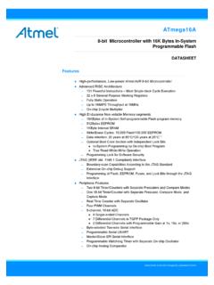
8 NXP Semiconductors 2021. All rights data sheetRev. 19 March 2021 5 of 82 NXP SemiconductorsLPC82x 32-bit ARM Cortex-M0+ microcontroller6. block diagram Gray-shaded blocks show peripherals that can provide hardware triggers or fixed DMA requests for DMA block diagramSRAM4/8 KBARMCORTEX-M0+TEST/DEBUGINTERFACEFLASH1 6/32 KBHIGH-SPEEDGPIOAHB TO APBBRIDGE CLOCKGENERATION,POWER CONTROL,SYSTEM FUNCTIONSRESET, CLKIN clocks and controlsLPC82xMaaa-014399slaveslaveslave ROMslaveCRCslavemasterPIN INTERRUPTS/PATTERN MATCHAHB-LITE BUSIRCWDOscBODPORSPI0/1 USART0/1/2 SDASCLSCT_PIN[3:0]29 x PIO029 x WWDTIOCONPMUSELFWAKE-UP TIMERMULTI-RATE TIMERI2C0/1/2/3 SCTIMER/PWMSWITCHMATRIXSCT_OUT[6:0]COMPA RATORXTALINXTALOUTACMP_OSYSCONRXD, CTSTXD, RTSACMP_I[4:1]VDDCMPADCADC_[11:0]SCK, SSELMISO, MOSIALWAYS-ON POWER DOMAINXTALSCLKCLKOUTSWCLK, SWDINPUT MUXDMALPC82xAll information provided in this document is subject to legal disclaimers.
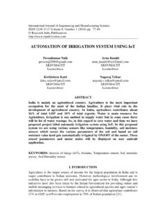
9 NXP Semiconductors 2021. All rights data sheetRev. 19 March 2021 6 of 82 NXP SemiconductorsLPC82x 32-bit ARM Cortex-M0+ microcontroller7. Pinning Pinning Fig 4. Pin configuration TSSOP20 packageTSSOP20 PIO0_23/ADC_3/ACMP_I4 PIO0_14/ADC_2/ACMP_I3 PIO0_17/ADC_9 PIO0_0/ACMP_I1/TDOPIO0_13/ADC_10 VREFPPIO0_12 VREFNRESET/PIO0_5 VSSPIO0_4/ADC_11/WAKEUP/TRSTVDDSWCLK/PIO 0_3/TCKPIO0_8/XTALINSWDIO/PIO0_2/TMSPIO0 _9/XTALOUTPIO0_11/I2C0_SDAPIO0_1/ACMP_I2 /CLKIN/TDIPIO0_10/I2C0_SCLPIO0_15aaa-011 3911234567891012111413161518172019 Fig 5. Pin configuration HVQFN33 packageaaa-011396 Transparent top viewPIO0_9/XTALOUTSWDIO/PIO0_2/TMSPIO0_1 1/I2C0_SDAPIO0_8/XTALINSWCLK/PIO0_3/TCKV DDPIO0_28/WKTCLKINVREFNPIO0_4/ADC_11/TRS TVREFPPIO0_5/RESETPIO0_7/ADC_0 PIO0_12 PIO0_6/ADC_1/VDDCMPPIO0_13/ADC_10 PIO0_0/ACMP_I1/TDOPIO0_10/I2C0_SCLPIO0_1 6 PIO0_27 PIO0_26 PIO0_25 PIO0_24 PIO0_15 PIO0_1/ACMP_I2/CLKIN/TDIPIO0_17/ADC_9 PIO0_18/ADC_8 PIO0_19/ADC_7 PIO0_20/ADC_6 PIO0_21/ADC_5 PIO0_22/ADC_4 PIO0_23/ADC_3/ACMP_I4 PIO0_14/ADC_2/ACMP_I38177186195204213222 231249101112131415163231302928272625term inal 1index area33 VSSLPC82xAll information provided in this document is subject to legal disclaimers.
10 NXP Semiconductors 2021. All rights data sheetRev. 19 March 2021 7 of 82 NXP SemiconductorsLPC82x 32-bit ARM Cortex-M0+ Pin descriptionThe pin description table Table 3 shows the pin functions that are fixed to specific pins on each package. These fixed-pin functions are selectable through the switch matrix between GPIO and the comparator, ADC, SWD, RESET, and the XTAL pins. By default, the GPIO function is selected except on pins PIO0_2, PIO0_3, and PIO0_5. JTAG functions are available in boundary scan mode function for the I2C, USART, SPI, and SCT pin functions can be assigned through the switch matrix to any pin that is not power or ground in place of the pin s fixed following exceptions apply:Do not assign more than one output to any pin. However, more than one input can be assigned to a pin. Once any function is assigned to a pin, the pin s GPIO functionality is PIO0_4 triggers a wake-up from Deep power-down mode.