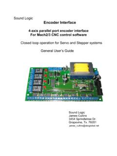
Transcription of LS7083 & LS7084 Encoder to Counter Interface Chips
1 LS7083 & LS7084 Encoder to Counter Interface Chips Description: These devices allow incremental shaft encoders to drive standard up/. down counters. Connect the Encoder quadrature outputs to the A & B. inputs. The LS7083 outputs can connect directly to the up and down clock inputs of counters such as 74193 or 40193. The LS7084 outputs can connect directly to the Clock and Up/Dn inputs of counters such as 4516 or 74169. Features: X4 or X1 resolution multiplication TTL and CMOS compatible Low power (micro-amps). 8-pin DIP or SOIC package No external clocks required Drive standard Up/Dn counters Monolithic CMOS. Pin Descriptions: Pin 1 (Rbias input): Connect a F bypass capacitor and resistor to ground for the internal current mirror which feeds the two internal 2-axis one-shots.
2 The resistor value sets the width of the low-true clock outputs. A typical value is 300kOhm which sets the output pulse width to 1 s and max A,B frequency to 250kHz. Minimum resistor value is 50kOhm. See the Rbias table (next page) for other values. The chip's current consumption is inversely proportional to this resistance. Typical current is 40 A @ 100 KOhm and 6 A @ 2 MegOhm. Pins 4 & 5 (A & B inputs): Connect to the A & B quadrature outputs of the Encoder . Both inputs have debounce filters. Minimum pulse width is set at 160ns. There is no maximum limit. Input current is less than 1 A. The A&B inputs can be swapped to reverse the direction of the external counters. Pin 6 (X4/X1 input): A high level applied to this input selects X4 mode, a low level selects the X1 mode.
3 Input current is less than 1 A. Do not let this input float. In X4 mode, a clock pulse is generated for every transition of the A or B input. Note that there are 4 transitions per cycle of quadrature code. Thus, a 500 cycle/rev Encoder will produce 2000 counts/rev in X4 mode. In X1 mode, only one clock is generated per quadrature cycle. LS7083 pin 7 (Down Clock output): Normally high, low-true. The low level pulse width is set by pin 1. Down counts are enabled only when B leads A (clockwise rotation). In X4 mode, one pulse is generated for each A/B state change. In X1 mode, one pulse is generated per quadrature cycle. LS7084 pin 7 (Up/Down Clock output): This output steers the external Counter up or down.
4 High = Up (A leads B), Low = Down (B leads A). LS7083 pin 8 (Up Clock output): Normally high, low-true. The low level pulse width is set by pin 1. Up counts are enabled only when A leads B ( Counter -clockwise rotation). In X4 mode, one pulse is generated for each A/B state change. In X1 mode, one pulse is generated per quadrature cycle. LS7084 pin 8 (Clock output): Normally high, low-true. The low level pulse width is set by pin 1. In X4 mode, one pulse is generated for each A/B state change regardless of count direction. In X1 mode, one pulse is generated per quadrature cycle. The external Counter should count on the rising (high-going) edge of this output. Surface Mount Package: The 8-pin SOIC package has the same pin-out as the DIP version shown above.
5 Absolute Maximum Ratings: DC Electrical Characteristics for 5V Operation: Parameter Min. Max. Units Parameter Min. Max. Units Notes Operating temperature 0 70 C Supply voltage Volts Storage temperature -65 150 C Supply current - A A,B = 0Hz Voltage at any input VCC+.5 Volts Rbias=300k Supply voltage (Vcc) Volts X4/X1 logic low Volts X4/X1 logic high Volts RBias Resistor Value vs. Timing: A,B logic low Volts Resistor Pulse Width Max A,B Freq A,B logic high Volts 100kOhm 400ns 625kHz Low output current mA Vout = 300kOhm 1 s 250kHz High output current mA Vout = 500kOhm s 180kHz use standard CMOS levels when operating with higher supply 2 MegOhm 5 s 50kHz voltages up to Volts.
6 10 MegOhm 25 s 10kHz phone: l sales: l fax: email: l website: page 11100 ne 34th circle l vancouver, washington 98682 USA 1. LS7083 & LS7084 Encoder to Counter Interface Chips LS7083 Timing Diagram: LS7084 Timing Diagram: Timing Diagram Notes: The maximum time delay from the A or B input to the leading edge of any output is 235ns. The pulse width of all clock outputs is set by the value of the Rbias resistor as shown in the table above. Typical rise or fall time of each logic output 10 to 20ns. Ordering Information: DIP Package (600mil): Price: LS7083 -DIP or $ / 1. LS7084 -DIP. $ / 25. $ / 100. SOIC Package: $ / 500. LS7083 -SOIC or $ / 1K. LS7084 -SOIC. Technical Data, Rev.
7 , August 2000. All Information subject to change without notice. phone: l sales: l fax: email: l website: page 11100 ne 34th circle l vancouver, washington 98682 USA 2.