Transcription of MAX3483E/MAX3485E/MAX3486E/MAX3488E/MAX3490E/MAX3491E …
1 General DescriptionDevices in the MAX3483E family (MAX3483E/MAX3485E/MAX3486E/MAX3488E/MAX 3490E/MAX3491E) are 15kV ESD- protected , + , low-power transceivers for RS-485 and RS-422 communications. Each device con-tains one driver and one receiver. The MAX3483E and MAX3488E feature slew -rate- limited drivers that minimize EMI and reduce reflections caused by improperly termi-nated cables, allowing error-free data transmission at data rates up to 250kbps. The partially slew -rate- limited MAX3486E transmits up to The MAX3485E, MAX3490E, and MAX3491E transmit at up to devices feature enhanced electrostatic discharge (ESD) protection. All transmitter outputs and receiver inputs are protected to 15kV using IEC 1000-4-2 Air-Gap Discharge, 8kV using IEC 1000-4-2 Contact Discharge, and 15kV using the Human Body are short-circuit current limited and are protected against excessive power dissipation by thermal shutdown circuitry that places the driver outputs into a high-impedance state.
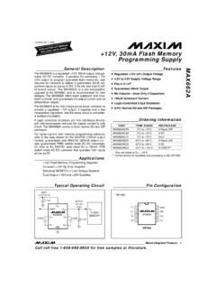
2 The receiver input has a fail-safe feature that guar-antees a logic-high output if both inputs are open MAX3488E, MAX3490E, and MAX3491E feature full-duplex communication, while the MAX3483E, MAX3485E, and MAX3486E are designed for half-duplex Telecommunications Industrial-Control Local Area Networks Transceivers for EMI-Sensitive Applications Integrated Services Digital Networks Packet SwitchingFeatures ESD Protection for RS-485 I/O Pins 15kV Human Body Model 8kV IEC 1000-4-2, Contact Discharge 15kV IEC 1000-4-2, Air-Gap Discharge Operate from a Single + Supply No Charge Pump Required Interoperable with +5V Logic Guaranteed 12 Mbps Data Rate (MAX3485E/MAX3490E/MAX3491E) slew -Rate limited for Errorless Data Transmission (MAX3483E/MAX3488E) 2nA Low-Current Shutdown Mode (MAX3483E/MAX3485E/MAX3486E/MAX3491E) -7V to +12V Common-Mode Input Voltage Range Full-Duplex and Half-Duplex Versions Available Industry-Standard 75176 Pinout (MAX3483E/MAX3485E/MAX3486E) Current-Limiting and Thermal Shutdown for Driver Overload Protection19-1474; Rev 1.
3 5/19 Ordering Information continued at end of data RANGEPIN-PACKAGEMAX3483 ECSA0 C to+70 C8 SOMAX3483 ECPA0 C to+70 C8 Plastic DIPMAX3483 EESA-40 C to+85 C8 SOMAX3483 EEPA-40 C to+85 C8 Plastic DIPPARTNUMBERGUARANTEEDDATA RATE(Mbps)SUPPLYVOLTAGE(V)HALF/FULLDUPLE XSLEW-RATELIMITEDDRIVER/RECEIVERENABLESH UTDOWNCURRENT(nA) 15kV ESD to sYe s2Ye s8 MAX3485E12 HalfNoYe s2Ye sYe s2Ye sNo Ye s8 MAX3490E12 FullNoNo Ye s8 MAX3491E12 FullNoYe s2Ye s14 MAX3483E/MAX3485E/MAX3486E/MAX3488E/MAX3 490 , 15kV ESD- protected , 12 Mbps and slew -Rate- limited True RS-485/RS-422 TransceiversSelector GuideOrdering InformationClick here for production status of specific part Voltage (VCC) ..+7 VControl Input Voltage (RE, DE).
4 To +7 VDriver Input Voltage (DI) .. to +7 VDriver Output Voltage (A, B, Y, Z) .. to + Input Voltage (A, B) .. to + Output Voltage (RO) .. to (VCC + )Continuous Power Dissipation (TA = +70 C) 8-Pin SO (derate C above +70 C) ..471mW 8-Pin Plastic DIP (derate C above +70 C) ..727mW14-Pin SO (derate C above +70 C) ..667mW14-Pin Plastic DIP (derate 10mW/ C above +70 C) ..800mWOperating Temperature Ranges MAX34_ _ EC_ _ ..0 C to +70 C MAX34_ _ EE_ _ ..-40 C to +85 CJunction Temperature ..+150 CStorage Temperature Range ..-65 C to +150 CLead Temperature (soldering, 10sec) ..+300 CTDFN-14 PACKAGE CODES14+1 Outline Number21-0041 Land Pattern Number90-0112 Thermal Resistance, Single-Layer Board:Junction to Ambient ( JA)120 C/WJunction to Case ( JC)37 C/WThermal Resistance, Four-Layer Board:Junction to Ambient ( JA)84 C/WJunction to Case ( JC)34 C/WPackage thermal resistances were obtained using the method described in JEDEC specification JESD51-7, using a four-layer board.
5 For detailed information on package thermal considerations, refer to the latest package outline information and land patterns (footprints), go to Note that a + , # , or - in the package code indicates RoHS status only. Package drawings may show a different suffix character, but the drawing pertains to the package regardless of RoHS Integrated 2 MAX3483E/MAX3485E/MAX3486E/MAX3488E/MAX3 490 , 15kV ESD- protected , 12 Mbps and slew -Rate- limited True RS-485/RS-422 TransceiversAbsolute Maximum RatingsStresses beyond those listed under Absolute Maximum Ratings may cause permanent damage to the device. These are stress ratings only, and functional operation of the device at these or any other conditions beyond those indicated in the operational sections of the specifications is not implied.
6 Exposure to absolute maximum rating conditions for extended periods may affect device reliability.(VCC = + , TA = TMIN to TMAX, unless otherwise noted. Typical values are at TA = +25 C.)PARAMETERSYMBOLCONDITIONSMINTYPMAXUNI TSD ifferential Driver OutputVODRL = 100 (RS-422), Figure = 54 (RS-485), Figure = 60 (RS-485), VCC = , Figure in Magnitude of DriverDifferential Output Voltage forComplementary Output States(Note 1) VODRL = 54 or 100 , Figure Common-Mode OutputVoltageVOCRL = 54 or 100 , Figure 43 VChange in Magnitude ofCommon-Mode Output Voltage (Note 1) VOCRL = 54 or 100 , Figure High VoltageVIHDE, DI, Low VoltageVILDE, DI, Input CurrentIIN1DE, DI, RE 2 AInput Current (A, B)IIN2DE = 0V,VCC = 0V or = = Leakage (Y, Z)IODE = 0V, RE = 0V,VCC = 0V or , MAX3491 EVOUT = 12V20 AVOUT = -7V-20 Output Leakage (Y, Z)
7 In Shutdown ModeIODE = 0V, RE = VCC,VCC = 0V or , MAX3491 EVOUT = 12V1 AVOUT = -7V-1 Receiver Differential Threshold VoltageVTH-7V VCM Input Hysteresis VTHVCM = 0V50mVReceiver Output High VoltageVOHIOUT = , VID = 200mV, Figure 6 VCC - Output Low VoltageVOLIOUT = , VID = 200mV, Figure (High Impedance)Output Current at ReceiverIOZRVCC = , 0V VOUT VCC 1 AReceiver Input ResistanceRIN-7V VCM 12V12k Supply Voltage Integrated 3 MAX3483E/MAX3485E/MAX3486E/MAX3488E/MAX3 490 , 15kV ESD- protected , 12 Mbps and slew -Rate- limited True RS-485/RS-422 TransceiversDC Electrical Characteristics(VCC = + , TA = +25 C.)(VCC = + , TA = TMIN to TMAX, unless otherwise noted. Typical values are at TA = +25 C)*MAX3488E and MAX3491E will be compliant to 8kV per IEC 1000-4-2 Contact Discharge by September CurrentICCNo load,DI = 0 or VCCDE = VCC, RE = 0 or = 0V, RE = Current in Shutdown ModeISHDNDE = 0, RE = VCC, DI = VCC or ADriver Short-Circuit OutputCurrentIOSDVOUT = -7V-250mAVOUT = 12V250 Receiver Short-Circuit OutputCurrentIOSR0 VRO VCC 8 60mAESD Protection for Y, Z, A, BIEC 1000-4-2 Air Discharge 15kVIEC 1000-4-2 Contact Discharge (MAX3483E, MAX3485E, MAX3486E, MAX3491E) 8 IEC 1000-4-2 Contact Discharge (MAX3490E, MAX3488E)
8 * 6 Human Body Model 15 PARAMETERSYMBOLCONDITIONSMINTYPMAXUNITSM aximum Data Rate1215 MbpsDriver Differential Output DelaytDDRL = 60 , Figure 712235nsDriver Differential Output Transition TimetTDRL = 60 , Figure 731125nsDriver Propagation Delay, Low-to-High LeveltPLHRL = 27 , Figure 872335nsDriver Propagation Delay, High-to-Low LeveltPHLRL = 27 , Figure 872335ns|tPLH - tPHL| Driver Propagation Delay Skew (Note 2)tPDSRL = 27 , Figure 8nsDRIVER-OUTPUT ENABLE/DISABLE TIMES (MAX3485E/MAX3491E only)Driver-Output Enable Time to Low LeveltPZLRL = 110 , Figure 104290nsDriver-Output Enable Time to High LeveltPZHRL = 110 , Figure 94290nsDriver-Output Disable Time from High LeveltPHZRL = 110 , Figure 93580nsDriver-Output Disable Time from Low LeveltPLZRL = 110 , Figure 103580nsDriver-Output Enable Time from Shutdown to Low LeveltPSLRL = 110 , Figure 10650900nsDriver-Output Enable Time from Shutdown to High LeveltPSHRL = 110 , Figure Integrated 4 MAX3483E/MAX3485E/MAX3486E/MAX3488E/MAX3 490 , 15kV ESD- protected , 12 Mbps and slew -Rate- limited True RS-485/RS-422 TransceiversDriver Switching Characteristics MAX3485E/MAX3490E/MAX3491 EDC Electrical Characteristics (continued)(VCC = + , TA = +25 C)
9 (VCC = + , TA = +25 C.)PARAMETERSYMBOLCONDITIONSMINTYPMAXUNI TSM aximum Data Differential Output DelaytDDRL = 60 , Figure 7204270nsDriver Differential Output Transition TimetTDRL = 60 , Figure 7152860nsDriver Propagation Delay, Low-to-High LeveltPLHRL = 27 , Figure 8204275nsDriver Propagation Delay, High-to-Low LeveltPHLRL = 27 , Figure 8204275ns|tPLH - tPHL| Driver Propagation Delay Skew (Note 2)tPDSRL = 27 , Figure 8-6 12nsDRIVER-OUTPUT ENABLE/DISABLE TIMESD river Output Enable Time to Low LeveltPZLRL = 110 , Figure 1052100nsDriver Output Enable Time to High LeveltPZHRL = 110 , Figure 952100nsDriver Output Disable Time from High LeveltPHZRL = 110 , Figure 94080nsDriver Output Disable Time from Low LeveltPLZRL = 110 , Figure 104080nsDriver Output Enable Time from Shutdown to Low LeveltPSLRL = 110 , Figure 107001000nsDriver Output Enable Time from Shutdown to High LeveltPSHRL = 110 , Figure 97001000nsPARAMETERSYMBOLCONDITIONSMINTY PMAXUNITSM aximum Data Rate250kbpsDriver Differential Output DelaytDDRL = 60 , Figure 76009001400nsDriver Differential Output Transition TimetTDRL = 60.
10 Figure 74007401200nsDriver Propagation Delay, Low-to-High LeveltPLHRL = 27 , Figure 87009301500nsDriver Propagation Delay, High-to-Low LeveltPHLRL = 27 , Figure 87009301500ns|tPLH - tPHL| Driver Propagation Delay Skew (Note 2)tPDSRL = 27 , Figure 8 50nsDRIVER-OUTPUT ENABLE/DISABLE TIMES (MAX3483E only)Driver-Output Enable Time to Low LeveltPZLRL = 110 , Figure 109001300nsDriver-Output Enable Time to High LeveltPZHRL = 110 , Figure 9600800nsDriver-Output Disable Time from High LeveltPHZRL = 110 , Figure 95080nsDriver-Output Disable Time from Low LeveltPLZRL = 110 , Figure 105080nsDriver-Output Enable Time from Shutdown to Low LeveltPSLRL = 110 , Figure sDriver-Output Enable Time from Shutdown to High LeveltPSHRL = 110 , Figure Integrated 5 MAX3483E/MAX3485E/MAX3486E/MAX3488E/MAX3 490 , 15kV ESD- protected , 12 Mbps and slew -Rate- limited True RS-485/RS-422 TransceiversDriver Switching Characteristics MAX3483E/MAX3488 EDriver Switching Characteristics MAX3486E(VCC = + , TA = +25 C)Note 1.