Transcription of MCP1700 Low Quiescent Current LDO Data Sheet
1 2005-2018 Microchip Technology 1 MCP1700 Features AEC-Q100 Qualified and PPAP Capable A Typical Quiescent Current Input Operating voltage Range: to Output voltage Range: to 250 mA Output Current for Output Voltages 200 mA Output Current for Output Voltages < Low dropout (LDO) voltage - 178 mV Typical @ 250 mA for VOUT= Typical Output voltage Tolerance Standard Output voltage Options:- , , , , , , , Stable with F Ceramic Output Capacitor Short Circuit Protection Overtemperature ProtectionApplications Battery-Powered Devices Battery-Powered Alarm Circuits Smoke Detectors CO2 Detectors Pagers and Cellular Phones Smart Battery Packs Low Quiescent Current voltage Reference PDAs Digital Cameras Microcontroller PowerRelated Literature AN765, Using Microchip s micropower LDOs (DS00765), Microchip Technology Inc.
2 , 2002 AN766, Pin-Compatible CMOS Upgrades to BiPolar LDOs (DS00766), Microchip Technology Inc., 2002 AN792, A Method to Determine How Much Power a SOT23 Can Dissipate in an Application (DS00792), Microchip Technology Inc., 2001 General DescriptionThe MCP1700 is a family of CMOS low dropout (LDO) voltage regulators that can deliver up to 250 mA ofcurrent while consuming only A of quiescentcurrent (typical). The input operating range is specifiedfrom to , making it an ideal choice for two andthree primary cell battery-powered applications, as wellas single cell Li-Ion-powered MCP1700 is capable of delivering 250 mA withonly 178 mV of input to output voltage differential(VOUT= ). The output voltage tolerance of theMCP1700 is typically at +25 C and 3%maximum over the operating junction temperaturerange of -40 C to +125 voltages available for the MCP1700 range to The LDO output is stable when using only1 F output capacitance.
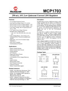
3 Ceramic, tantalum oraluminum electrolytic capacitors can all be used forinput and output. Overcurrent limit and overtemperatureshutdown provide a robust solution for any options include SOT-23, SOT-89, TO-92 and2x2 Types132 VINGND VOUTMCP1700123 VINGNDVOUTMCP17003-Pin SOT-233-Pin SOT-89321 GND VINVOUTMCP17003-Pin TO-92 VINVIN123EP7* Includes Exposed Thermal Pad (EP); see Table DFN-6*Low Quiescent Current LDO 2005-2018 Microchip Technology 2 MCP1700 Functional Block DiagramsTypical Application Circuits+-VINVOUTGND+VINE rror AmplifierVoltageReferenceOvercurrentOver temperatureMCP1700 GNDVOUTVINCIN1 F CeramicCOUT1 F CeramicVOUTVIN( to ) mAMCP1700 2005-2018 Microchip Technology CHARACTERISTICSA bsolute Maximum Ratings + inputs and outputs .. (VSS- ) to (VIN+ )Peak Output Current .
4 Internally LimitedStorage Temperature ..-65 C to +150 CMaximum Junction Temperature .. 150 COperating Junction C to +125 CESD protection on all pins (HBM;MM) 4kV; 400V Notice: Stresses above those listed under MaximumRatings may cause permanent damage to the device. This isa stress rating only, and functional operation of the device atthose or any other conditions above those indicated in theoperational listings of this specification is not to maximum rating conditions for extended periodsmay affect device reliability. DC CHARACTERISTICSE lectrical Characteristics: Unless otherwise specified, all limits are established for VIN=VR+1V, ILOAD= 100 A,COUT=1 F (X7R), CIN=1 F(X7R), TA= +25 type applies for junction temperatures, TJ (Note 6) of -40 C to +125 CharacteristicsInput Operating 1 Input Quiescent CurrentIq AIL=0mA, VIN=VR+1 VMaximum Output CurrentIOUT_mA250200 mAFor VR VR Short Circuit CurrentIOUT_SC 408 mAVIN=VR+1V, VOUT=GNDC urrent (peak Current ) measured 10 ms after short is voltage VR+ + 2 VOUT Temperature CoefficientTCVOUT 50 ppm/ CNote 3 Line Regulation VOUT/(VOUTX VIN) + (VR+1)V VIN 6 VLoad Regulation + mA to 250 mA for VR mA to 200 mA for VR 4 dropout VoltageVR 178350mVIL= 250 mA, (Note 1, Note 5) dropout VoltageVR 150350mVIL= 200 mA, (Note 1, Note 5)
5 Output Rise TimeTR 500 s10% VR to 90% VR VIN= 0V to 6V, RL=50 resistiveNote 1:The minimum VIN must meet two conditions: VIN and VIN VR+ :VR is the nominal regulator output voltage . For example: VR= , , , , , , , , , The input voltage VIN=VR+ ; IOUT= 100 :TCVOUT=(VOUT-HIGH-VOUT-LOW) *106 / (VR* Temperature), VOUT-HIGH= highest voltage measured over the temperature range. VOUT-LOW= lowest voltage measured over the temperature :Load regulation is measured at a constant junction temperature using low duty cycle pulse testing. Changes in output voltage due to heating effects are determined using thermal regulation specification : dropout voltage is defined as the input to output differential at which the output voltage drops 2% below its measured value with a VR+ 1V differential :The maximum allowable power dissipation is a function of ambient temperature, the maximum allowable junction temperature and the thermal resistance from junction to air ( TA, TJ, JA).
6 Exceeding the maximum allowable power dissipation will cause the device operating junction temperature to exceed the maximum 150 C rating. Sustained junction temperatures above 150 C can impact the device :The junction temperature is approximated by soaking the device under test at an ambient temperature equal to the desired Junction temperature. The test time is small enough such that the rise in the Junction temperature over the ambient temperature is not significant. 2005-2018 Microchip Technology 4 MCP1700 Output NoiseeN 3 V/(Hz)1/2IL= 100 mA, f = 1 kHz, COUT=1 FPower Supply Ripple Rejection RatioPSRR 44 dBf = 100 Hz, COUT=1 F, IL=50mA, VINAC= 100 mV pk-pk, CIN=0 F, VR= Shutdown ProtectionTSD 140 CVIN=VR+1V, IL= 100 ATEMPERATURE SPECIFICATIONSE lectrical Characteristics: Unless otherwise specified, all limits are established for VIN=VR+1V, ILOAD= 100 A,COUT=1 F (X7R), CIN=1 F (X7R), TA= +25 type applies for junction temperatures, TJ (Note 1) of -40 C to +125 RangesSpecified Temperature RangeTA-40+125 COperating Temperature RangeTJ-40+125 CStorage Temperature RangeTA-65+150 CThermal Package ResistanceThermal Resistance, 2x2 DFN JA 91 C/WEIA/JEDEC JESD51-7FR-4 4-Layer Board JC(Top) 286 C/W JC(Bottom) C/W JT C/WThermal Resistance, SOT-23 JA 212 C/WEIA/JEDEC JESD51-7FR-4 4-Layer Board JC(Top) 139 C/W JC(Bottom) C/W JT C/WThermal Resistance, SOT-89 JA 104 C/WEIA/JEDEC JESD51-7FR-4 4-Layer Board JC(Top) 74 C/W JT 30 C/WNote 1.
7 The maximum allowable power dissipation is a function of ambient temperature, the maximum allowable junctiontemperature and the thermal resistance from junction to air ( TA, TJ, JA). Exceeding the maximum allowable powerdissipation will cause the device operating junction temperature to exceed the maximum 150 C rating. Sustainedjunction temperatures above 150 C can impact the device reliability. DC CHARACTERISTICS (CONTINUED)Electrical Characteristics: Unless otherwise specified, all limits are established for VIN=VR+1V, ILOAD= 100 A,COUT=1 F (X7R), CIN=1 F(X7R), TA= +25 type applies for junction temperatures, TJ (Note 6) of -40 C to +125 1:The minimum VIN must meet two conditions: VIN and VIN VR+ :VR is the nominal regulator output voltage . For example: VR= , , , , , , , , , The input voltage VIN=VR+ ; IOUT= 100 :TCVOUT=(VOUT-HIGH-VOUT-LOW) *106 / (VR* Temperature), VOUT-HIGH= highest voltage measured over the temperature range.
8 VOUT-LOW= lowest voltage measured over the temperature :Load regulation is measured at a constant junction temperature using low duty cycle pulse testing. Changes in output voltage due to heating effects are determined using thermal regulation specification : dropout voltage is defined as the input to output differential at which the output voltage drops 2% below its measured value with a VR+ 1V differential :The maximum allowable power dissipation is a function of ambient temperature, the maximum allowable junction temperature and the thermal resistance from junction to air ( TA, TJ, JA). Exceeding the maximum allowable power dissipation will cause the device operating junction temperature to exceed the maximum 150 C rating. Sustained junction temperatures above 150 C can impact the device :The junction temperature is approximated by soaking the device under test at an ambient temperature equal to the desired Junction temperature.
9 The test time is small enough such that the rise in the Junction temperature over the ambient temperature is not significant. 2005-2018 Microchip Technology 5 MCP1700 Thermal Resistance, TO-92 JA 92 C/WEIA/JEDEC JESD51-7FR-4 4-Layer Board JC(Top) 74 C/WTEMPERATURE SPECIFICATIONS (CONTINUED)Electrical Characteristics: Unless otherwise specified, all limits are established for VIN=VR+1V, ILOAD= 100 A,COUT=1 F (X7R), CIN=1 F (X7R), TA= +25 type applies for junction temperatures, TJ (Note 1) of -40 C to +125 1:The maximum allowable power dissipation is a function of ambient temperature, the maximum allowable junctiontemperature and the thermal resistance from junction to air ( TA, TJ, JA). Exceeding the maximum allowable powerdissipation will cause the device operating junction temperature to exceed the maximum 150 C rating.
10 Sustainedjunction temperatures above 150 C can impact the device reliability. 2005-2018 Microchip Technology PERFORMANCE CURVESNote: Unless otherwise indicated: VR= , COUT= 1 F Ceramic (X7R), CIN= 1 F Ceramic (X7R), IL= 100 A,TA= +25 C, VIN=VR+ : Junction Temperature (TJ) is approximated by soaking the device under test to an ambient temperature equal to the desired junctiontemperature. The test time is small enough such that the rise in Junction temperature over the Ambient temperature is not 2-1:Input Quiescent Current vs. Input 2-2:Ground Current vs. Load 2-3: Quiescent Current vs. Junction 2-4:Output voltage vs. Input voltage (VR= ).FIGURE 2-5:Output voltage vs. Input voltage (VR= ).FIGURE 2-6:Output voltage vs. Input voltage (VR= ).Note:The graphs and tables provided following this note are a statistical summary based on a limited number ofsamples and are provided for informational purposes only.