Transcription of MCP23016 16-Bit I2C I/O Expander - Microchip Technology
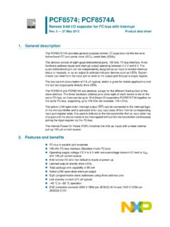
1 2007 Microchip Technology 1 MCP23016 Features 16-Bit remote bidirectional I/O port- 16 I/O pins default to 16 inputs Fast i2c bus clock frequency (0 - 400 kbits/s) Three hardware address pins allow use of up to eight devices High-current drive capability per I/O: 25 mA Open-drain interrupt output on input change Interrupt port capture register Internal Power-On Reset (POR) Polarity inversion register to configure the polarity of the input port data Compatible with most microcontrollers Available temperature range:- Industrial (I): -40 C to +85 CCMOS Technology Operating Supply Voltage: to Low standby currentPackages 28-pin PDIP, 300 mil; 28-pin SOIC, 300 mil 28-pin SSOP, 209 mil.
2 28-pin QFN, 6x6 mm Package TypesBlock 1234567891011121314282726252423222120191 8171615 PDIP, SOIC, 118 912 1314 MCP23016 MCP2301616 to to pulseRead pulseLow PassFilterInterruptLogicI2C BusControlAddressDecoderPower-onResetI/O PortDeserializerSerializer/ControlClockG enI2C BusInterface/ProtocolHandlerINTA0A1A2 SCLSDACLKINVDDVSSC onfigurationRegistersControl8-BitTPIARES 16-Bit I2C I/O ExpanderMCP23016DS20090C-page 2 2007 Microchip Technology : 2007 Microchip Technology OVERVIEWThe MCP23016 device provides 16-Bit , generalpurpose, parallel I/O expansion for I2C device includes high-current drive capability, lowsupply current and individual I/O configuration.
3 I/Oexpanders provide a simple solution when additionalI/Os are needed for ACPI, power switches, sensors,push buttons, LEDs and so MCP23016 consists of multiple 8-bit configurationregisters for input, output and polarity selection. Thesystem master can enable the I/Os as either inputs oroutputs by writing the I/O configuration bits. The datafor each input or output is kept in the correspondinginput or output register. The polarity of the read registercan be inverted with the polarity inversion register (seeSection , Input Polarity Registers ). Allregisters can be read by the system open-drain interrupt output is activated when anyinput state differs from its corresponding input portregister state.
4 This is used to indicate to the systemmaster that an input state has changed. The interruptcapture register captures port value at this time. ThePower-on Reset sets the registers to their default val-ues and initializes the device state device inputs (A0 - A2) determine the I2 Caddress and allow up to eight I/O Expander devices toshare the same I2C DescriptionsTABLE 1-1:PINOUT DESCRIPTION Pin NamePDIP,SOIC,SSOPPin source inputTP107O Test Pin (This pin must be left floating) digital input/output for digital input/output for digital input/output for digital input/output for digital input/output for digital input/output for digital input/output for digital input/output for digital input/output for digital input/output for digital input/output for digital input/output for digital input/output for digital input/output for digital input/output for digital input/output for GP0 SCL1411 ISTS erial clock inputSDA1512I/OSTS erial data I/OINT63 OODI nterrupt outputA01613 ISTA ddress input 1A11714 ISTA ddress input 2A21815 ISTA ddress input 3 VSS1, 8, 195, 16.
5 26P Ground reference for logic and I/O pinsVDD2017P Positive supply for logic and I/O pinsMCP23016DS20090C-page 4 2007 Microchip Technology Reset (POR)The on-chip POR circuit holds the chip in RESET untilVDD has reached a high enough level to deactivate thePOR circuit ( , release RESET). A maximum risetime for VDD is specified in the electrical the device starts normal operation (exits theRESET condition), device operating parameters(voltage, frequency, temperature) must be met toensure proper Timer (PWRT)The Power-up Timer provides a 72 ms nominal time-out on power-up, keeping the device in RESET andallowing VDD to rise to an acceptable power-up time delay will vary from chip-to-chip dueto VDD, temperature and process variation.
6 SeeTable 2-4 for details (TPWRT, parameter 3). GeneratorThe MCP23016 uses an external RC circuit todetermine the internal clock speed. The user mustconnect R and C to the MCP23016 , as shown inFigure 1-1:CLOCK CONFIGURATIONA 1 MHz (typ.) internal clock is needed for the device tofunction properly. The internal clock can be measuredon the TP pin. Recommended REXT and CEXT valuesare shown in Table Bus Interface/ Protocol HandlerThis block manages the functionality of the I2C businterface and protocol handling. The MCP23016supports the following commands:TABLE 1-3:COMMAND BYTE TO REGISTER DecoderThe last three LSb of the 7-bit address are user-defined(see Table 1-4).
7 Three hardware pins (<A2:A0>) definethese 1-4:DEVICE ADDRESSI nternal ClockMCP23016 VDDREXTCEXTVSSCLKNote:Set IARES = 1 to measure the clockoutput on 1-2:RECOMMENDED k 33 pFCommand ByteResult0hAccess to GP01hAccess to GP12hAccess to OLAT03hAccess to OLAT14hAccess to IPOL05hAccess to IPOL16hAccess to IODIR07hAccess to IODIR18hAccess to INTCAP0 (Read-Only)9hAccess to INTCAP1 (Read-Only)AhAccess to IOCON0 BhAccess to IOCON10100A2A1A0 2007 Microchip Technology BlockThe register block contains the Configuration and Port registers, as shown in Table 1-5:REGISTER SUMMARYNameBit 7 Bit 6 Bit 5 Bit 4 Bit 3 Bit 2 Bit 1 Bit 0 Value onPORPort 0000 Configuration xxxxIOCON0 IARES---- ---0 IOCON1 IARES---- ---0 Legend: 1 bit is set, 0 bit is cleared, x = unknown, = 6 2007 Microchip Technology PORT REGISTERSTwo registers provide access to the two GPIO ports: GP0 (provides access to data port GP0) GP1 (provides access to data port GP1)A read from this register provides status on pins ofthese ports.
8 A write to these registers will modify theoutput latch registers (OLAT0, OLAT1) and data 1-1:GP0 - GENERAL PURPOSE I/O PORT REGISTER 0 REGISTER 1-2:GP1 - GENERAL PURPOSE I/O PORT REGISTER 1 R/W-0R/W-0R/W-0R/W-0R/W-0R/W-0R/W-0 7bit 0bit : Reflects the logic level on the = Logic 1 0 = Logic 0 Legend:R = Readable bitW = Writable bitU = Unimplemented bit, read as 0 - n = Value at POR 1 = Bit is set 0 = Bit is clearedx = Bit is unknownR/W-0R/W-0R/W-0R/W-0R/W-0R/W-0R/W -0 7bit 0bit : Reflects the logic level on the = Logic 1 0 = Logic 0 Legend:R = Readable bitW = Writable bitU = Unimplemented bit, read as 0 - n = Value at POR 1 = Bit is set 0 = Bit is clearedx = Bit is unknown 2007 Microchip Technology LATCH REGISTERSTwo registers provide access to the two port outputlatches: OLAT0 (provides access to the output latch for port GP0) OLAT1 (provides access to the output latch for port GP1)A read from these registers results in a read of the latchthat controls the output and not the actual port.
9 A writeto these registers updates the output latch that controlsthe 1-3:OLAT0 - OUTPUT LATCH REGISTER 0 REGISTER 1-4: OLAT1 - OUTPUT LATCH REGISTER 1 R/W-0R/W-0R/W-0R/W-0R/W-0R/W-0R/W-0 7bit 0bit : Reflects the logic level on the output = Logic 1 0 = Logic 0 Legend:R = Readable bitW = Writable bitU = Unimplemented bit, read as 0 - n = Value at POR 1 = Bit is set 0 = Bit is clearedx = Bit is unknownR/W-0R/W-0R/W-0R/W-0R/W-0R/W-0R/W -0 7bit 0bit : Reflects the logic level on the output = Logic 1 0 = Logic 0 Legend:R = Readable bitW = Writable bitU = Unimplemented bit, read as 0 - n = Value at POR 1 = Bit is set 0 = Bit is clearedx = Bit is unknownMCP23016DS20090C-page 8 2007 Microchip Technology POLARITY REGISTERST hese registers allow the user to configure the polarityof the input port data (GP0 and GP1).
10 If a bit in this reg-ister is set, the corresponding input port (GPn) data bitpolarity will be inverted. IPOL0 (controls the polarity of GP0) IPOL1 (controls the polarity of GP1)REGISTER 1-5:IPOL0 - INPUT POLARITY PORT REGISTER 0 REGISTER 1-6:IPOL1 - INPUT POLARITY PORT REGISTER 1 R/W-0R/W-0R/W-0R/W-0R/W-0R/W-0R/W-0 7bit 0bit : Controls the polarity inversion for the input pins1 = Corresponding GP0 bit is inverted0 = Corresponding GP0 bit is not invertedLegend:R = Readable bitW = Writable bitU = Unimplemented bit, read as 0 - n = Value at POR 1 = Bit is set 0 = Bit is clearedx = Bit is unknownR/W-0R/W-0R/W-0R/W-0R/W-0R/W-0R/W -0 7bit 0bit : Controls the polarity inversion for the input pins1 = Corresponding GP1 bit is inverted0 = Corresponding GP1 bit is not invertedLegend.