Transcription of MCP23017/MCP23S17 Data Sheet - Microchip Technology
1 2005-2016 Microchip Technology 1 MCP23017/MCP23S17 Features 16-Bit Remote Bidirectional I/O Port:- I/O pins default to input High-Speed I2C interface ( mcp23017 ) High-Speed SPI interface (MCP23S17):- 10 MHz (maximum) Three Hardware Address Pins to Allow Up to Eight Devices On the Bus Configurable Interrupt Output Pins:- Configurable as active-high, active-low or open-drain INTA and INTB Can Be Configured to Operate Independently or Together Configurable Interrupt Source:- Interrupt-on-change from configured register defaults or pin changes Polarity Inversion Register to Configure the Polarity of the Input Port Data External Reset Input Low Standby Current: 1 A (max.)
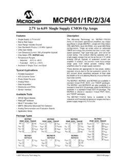
2 Operating Voltage:- to @ -40 C to +85 C- to @ -40 C to +85 C- to @ -40 C to +125 CPackages 28-pin QFN, 6 x 6 mm Body 28-pin SOIC, Wide, mm Body 28-pin SPDIP, 300 mil Body 28-pin SSOP, mm BodyPackage Types2345617 VSSNC15161718192021 GPA4 GPA3 GPA2 GPA1 GPA0 VDDINTBSCKSDANCA0A1A2 RESET23242526272822 GPB3 GPB2 GPB1 GPB0 GPA7 GPA6 GPA510 118 9121314 GPB5 GPB6 GPB7 GPB4 INTAGPB0 GPB1 GPB2 GPB3 INTAGPB4 NCNCGPB5 GPB6 GPB7 SCKGPA7 GPA6 GPA5 GPA4 GPA3 GPA2 GPA1 GPA0 VDDVSSA2A1A0 SDA 1234567891011121314282726252423222120191 8171615 INTBRESETEP29 *SPDIPSSOPSOICQFN* Includes Exposed Thermal Pad; see Ta b l e 2 - 118 9121314 GPB5 GPB6 GPB7 GPB4 INTASCKEP29 *GPB0 GPB1 GPB2 GPB3 INTAGPB4 SOCSGPB5 GPB6 GPB7 SCKGPA7 GPA6 GPA5 GPA4 GPA3 GPA2 GPA1 GPA0 VDDVSSA2A1A0SI 1234567891011121314282726252423222120191 8171615 INTBRESETMCP23S17 MCP2301716-Bit I/O Expander with serial InterfaceMCP23017/MCP23S17DS20001952C-pa ge 2 2005-2016 Microchip Technology Block DiagramGPB7 GPB6 GPB5 GPB4 GPB3 GPB2 GPB1 GPB0I2C ControlGPIOSCLSDARESETINTA16 Configuration/8A2.
3 A03 ControlRegistersSPI SISOSCKCSMCP23S17 mcp23017 GPA7 GPA6 GPA5 GPA4 GPA3 GPA2 GPA1 GPA0 INTBI nterruptGPIOS erializer/DeserializerLogicDecode 2005-2016 Microchip Technology 3 mcp23017 CHARACTERISTICSA bsolute Maximum Ratings Ambient temperature under -40 C to +125 CStorage temperature .. -65 C to +150 CVoltage on VDD with respect to VSS .. to + on all other pins with respect to VSS (except VDD).. to (VDD + )Total power 700 mWMaximum current out of VSS pin ..150 mAMaximum current into VDD pin .. 125 mAInput clamp current, IIK (VI < 0 or VI > VDD) .. 20 mAOutput clamp current, IOK (VO < 0 or VO > VDD).
4 20 mAMaximum output current sunk by any output pin .. 25 mAMaximum output current sourced by any output pin ..25 mAESD protection on all pins (HBM:MM) ..4 kV:400V Notice: Stresses above those listed under Maximum Ratings may cause permanent damage to the device. This isa stress rating only and functional operation of the device at those or any other conditions above those indicated in theoperational listings of this specification is not implied. Exposure to maximum rating conditions for extended periods mayaffect device 4 2005-2016 Microchip Technology CharacteristicsTABLE 1-1:DC CHARACTERISTICSE lectrical Specifications: Unless otherwise noted, VDD at -40 C TA +125 CParam.
5 (1) Start Voltage to ensure Power-on ResetVPOR VSS VD003 VDD Rise Rate to ensure Power-on V/msDesign guidance CurrentIDD 1mASCL/SCK = 1 MHzD005 Standby currentIDDS8 1 A-40 C TA +85 C 3 VDD +85 C TA +125 C (Note 1)Input Low VoltageD030A0, A1, A2 (TTL buffer)VILVSS , GPIO, SCL/SCK, SDA, RESET(Schmitt Trigger)VILVSS High VoltageD040A0, A1, A2 (TTL buffer) VDD + VDDVD041CS, GPIO, SCL/SCK, SDA, RESET(Schmitt Trigger) VDD VDDVFor entire VDD rangeInput Leakage CurrentD060I/O port pinsIIL 1 AVSS VPIN VDDO utput Leakage CurrentD065I/O port pinsILO 1 AVSS VPIN VDDD070 GPIO weak pull-up current IPU4075115 AVDD = 5 VGP pins = VSSO utput Low-VoltageD080 GPIOVOL = mAVDD = INTVOL = mAVDD = , SDAVOL = mAVDD = = mAVDD = High-VoltageD090 GPIO, INT, SOVOHVDD VIOH = mAVDD = IOH = -400 AVDD = Capacitive Loading Specs on Output PinsD101 GPIO, SO, INTCIO 50pFD102 SDACB 400pFNote 1:This parameter is characterized, not 100% tested.
6 2005-2016 Microchip Technology 5 mcp23017 CharacteristicsFIGURE 1-1:LOAD CONDITIONS FOR DEVICE TIMING SPECIFICATIONSFIGURE 1-2:RESET AND DEVICE RESET TIMER TIMINGTABLE 1-2:DEVICE RESET SPECIFICATIONSAC Characteristics: Unless otherwise noted, VDD at -40 C TA +125 (1) Pulse Width (Low)TRSTL1 s32 Device Active After Reset highTHLD 0 nsVDD = High-Impedance From RESET LowTIOZ 1 sNote 1:This parameter is characterized, not 100% pF1k VDDSCL andSDA pinMCP2301750 pFPinVDDRESETI nternalRESET34 Output pin3230 mcp23017 /MCP23S17DS20001952C-page 6 2005-2016 Microchip Technology 1-3:I2C BUS START/STOP BITS TIMINGFIGURE 1-4:I2C BUS DATA TIMINGTABLE 1-3:I2C BUS DATA REQUIREMENTSI2C interface AC Characteristics: Unless otherwise noted, VDD at -40 C TA +125 C, RPU (SCL, SDA) = 1 k , CL (SCL, SDA) = 135 pFParam.
7 Max. UnitsConditions100 Clock High Time:THIGH100 kHz kHz MHz Low Time:TLOW100 kHz kHz MHz and SCL Rise Time:TR (1)100 kHz mode kHz mode20 + CB (2) MHz mode20 and SCL Fall Time:TF (1)100 kHz mode kHz mode20 + CB (2) MHz mode20 1:This parameter is characterized, not 100% :CB is specified to be from 10 to 400 2005-2016 Microchip Technology 7 mcp23017 /MCP23S1790 START Condition Setup Time:TSU:STA100 kHz 400 kHz MHz Condition Hold Time:THD:STA100 kHz kHz MHz Input Hold Time:THD:DAT100 kHz mode 0 kHz mode0 MHz mode0 Input Setup Time:TSU:DAT100 kHz mode250 kHz mode100 MHz Condition Setup Time:TSU:STO100 kHz kHz MHz Valid From Clock:TAA100 kHz mode kHz mode MHz mode Free Time:TBUF100 kHz kHz MHz modeN/A N/A Capacitive Loading:CB100 kHz and 400 kHz 400pF Note MHz 100pFNote 1112 Input Filter Spike Suppression (SDA and SCL):TSP100 kHz and 400 kHz MHz 10nsSpike suppression offTABLE 1-3.
8 I2C BUS DATA REQUIREMENTS (CONTINUED)I2C interface AC Characteristics: Unless otherwise noted, VDD at -40 C TA +125 C, RPU (SCL, SDA) = 1 k , CL (SCL, SDA) = 135 pFParam. Max. UnitsConditionsNote 1:This parameter is characterized, not 100% :CB is specified to be from 10 to 400 8 2005-2016 Microchip Technology 1-5:SPI INPUT TIMINGFIGURE 1-6:SPI OUTPUT TIMINGTABLE 1-4:SPI interface REQUIREMENTSSPI interface AC Characteristics: Unless otherwise noted, VDD at -40 C TA +125 Clock FrequencyFCLK 1CS Setup TimeTCSS50 ns2CS Hold TimeTCSH100 Disable TimeTCSD100 50 Setup TimeTSU20 1:This parameter is characterized, not 100% inMSB inHigh-Impedance11 Mode 1,1 Mode 0,0 Note 1.
9 When using SPI Mode 1,1 the CS pin needs to be toggled once before the first communication (1)CSSCKSO813 MSB outLSB out214 Don t CareSIMode 1,1 Mode 0,0912 2005-2016 Microchip Technology 9 MCP23017/MCP23S17 FIGURE 1-7:GPIO AND INT TIMING5 Data Hold TimeTHD20 Rise TimeTR 2 sNote 17 CLK Fall TimeTF 2 sNote 18 Clock High TimeTHI90 Low TimeTLO90 Delay TimeTCLD50 ns11 Clock Enable TimeTCLE50 ns12 Output Valid from Clock LowTV Hold TimeTHO0 ns14 Output Disable TimeTDIS 100nsTABLE 1-4:SPI interface REQUIREMENTS (CONTINUED)SPI interface AC Characteristics: Unless otherwise noted, VDD at -40 C TA +125 1:This parameter is characterized, not 100% of data byte zeroduring a write or readINTPinINT Pin Active51command, dependingon parameterOutputGPnPinInputInactive5352 RegisterLoadedMCP23017/MCP23S17DS2000195 2C-page 10 2005-2016 Microchip Technology 1-5:GP AND INT PINS REQUIREMENTSGP and INT Pins AC Characteristics.
10 Unless otherwise noted, VDD at -40 C TA +125 Data to Output ValidTGPOV 500ns51 Interrupt Pin Disable TimeTINTD 600ns52GP Input Change to Register ValidTGPIV 450ns53 IOC Event to INT ActiveTGPINT 600nsGlitch Filter on GP PinsTGLITCH 150nsNote 1 Note 1:This parameter is characterized, not 100% tested. 2005-2016 Microchip Technology 11 mcp23017 DESCRIPTIONSThe descriptions of the pins are listed in Ta b l e 2 - 2-1:PINOUT DESCRIPTIONPinNameQFNSOICSPDIPSSOPPinTyp eFunctionGPB0251I/OBidirectional I/O pin. Can be enabled for interrupt-on-change and/or internal weak pull-up I/O pin. Can be enabled for interrupt-on-change and/or internal weak pull-up I/O pin.
