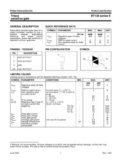
Transcription of MCR100 - Sensitive Gate Rectifiers
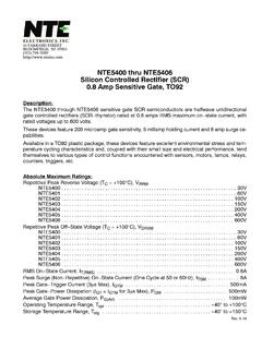
1 Semiconductor Components Industries, LLC, 2010 February, 2010 Rev. 101 Publication Order Number: MCR100 /DMCR100 SeriesSensitive GateSilicon Controlled RectifiersReverse Blocking ThyristorsPNPN devices designed for high volume, line-powered consumerapplications such as relay and lamp drivers, small motor controls, gatedrivers for larger thyristors, and sensing and detection in an inexpensive plastic TO-226AA package which isreadily adaptable for use in automatic insertion Sensitive gate Allows Triggering by Microcontrollers and OtherLogic Circuits Blocking Voltage to 600 V On State Current Rating of A RMS at 80 C High Surge Current Capability 10 A Minimum and Maximum Values of IGT, VGT and IH Specifiedfor Ease of Design Immunity to dV/dt 20 V/msec Minimum at 110 C Glass-Passivated Surface for Reliability and Uniformity Pb Free Packages are Available**For additional information on our Pb Free strategy and soldering details.
2 Pleasedownload the ON Semiconductor Soldering and Mounting TechniquesReference Manual, A RMS100 thru 600 VTO 92 CASE 29 STYLE 10 PIN ASSIGNMENT123 GateAnodeCathodeKGASee detailed ordering and shipping information on page 5 ofthis data Specific Device CodeA= Assembly LocationY= YearWW = Work WeekG= Pb Free PackageMARKING DIAGRAMMCR100 xAYWWGG12312 BENT LEADTAPE & REELAMMO PACKSTRAIGHT LEADBULK PACK3(Note: Microdot may be in either location) MCR100 RATINGS (TJ = 25 C unless otherwise noted)RatingSymbolValueUnitPeak Repetitive Off State Voltage (Notes 1 and 2)(TJ = *40 to 110 C, Sine Wave, 50 to 60 Hz; RGK = 1 kW) MCR100 3 MCR100 4 MCR100 6 MCR100 8 VDRM,VRRM100200400600 VOn-State RMS Current, (TC = 80 C) 180 Conduction AnglesIT(RMS) Non-Repetitive Surge Current, (1/2 Cycle, Sine Wave, 60 Hz, TJ = 25 C)ITSM10 ACircuit Fusing Consideration, (t = ms) Peak gate Power, (TA = 25 C, Pulse Width v ms) Average gate Power, (TA = 25 C, t = ms)PG(AV) Peak gate Current, (TA = 25 C, Pulse Width v ms) Peak gate Voltage, (TA = 25 C, Pulse Width v ms) Junction Temperature Range @ Rate VRRM and VDRMTJ 40 to 110 CStorage Temperature RangeTstg 40 to 150 CStresses exceeding Maximum Ratings may damage the device.
3 Maximum Ratings are stress ratings only. Functional operation above theRecommended Operating Conditions is not implied. Extended exposure to stresses above the Recommended Operating Conditions may affectdevice VDRM and VRRM for all types can be applied on a continuous basis. Ratings apply for zero or negative gate voltage; however, positive gatevoltage shall not be applied concurrent with negative potential on the anode. Blocking voltages shall not be tested with a constant currentsource such that the voltage ratings of the devices are See ordering information for exact device number CHARACTERISTICSC haracteristicSymbolMaxUnitThermal Resistance,Junction to CaseJunction to AmbientRqJCRqJA75200 C/WLead Solder Temperature(t1/16 from case, 10 secs max)TL260 CELECTRICAL CHARACTERISTICS (TC = 25 C unless otherwise noted)CharacteristicSymbolMinTypMaxUnitO FF CHARACTERISTICSPeak Repetitive Forward or Reverse Blocking Current (Note 3)TC = 25 C(VD = Rated VDRM and VRRM.)
4 RGK = 1 kW)TC = 110 CIDRM, IRRM 10100mAON CHARACTERISTICSPeak Forward On State Voltage*(ITM = A Peak @ TA = 25 C)VTM Trigger Current (Note 4)TC = 25 C(VAK = Vdc, RL = 100 W)IGT 40200mAHolding Current (Note 3)TC = 25 C(VAK = Vdc, Initiating Current = 20 mA, RGK = 1 kW)TC = 40 CIH Current (Note 4)TC = 25 C(VAK = V, Ig = 200 mA)TC = 40 CIL 1015mAGate Trigger Voltage (Note 4)TC = 25 C(VAK = Vdc, RL = 100 W)TC = 40 CVGT CHARACTERISTICSC ritical Rate of Rise of Off State Voltage(VD = Rated VDRM, Exponential Waveform, RGK = 1 kW,TJ = 110 C)dV/dt2035 V/msCritical Rate of Rise of On State Current(IPK = 20 A; Pw = 10 msec; diG/dt = 1 A/msec, Igt = 20 mA)di/dt 50A/ms*Indicates Pulse Test: Pulse Width ms, Duty Cycle 1%.3. RGK = 1000 W included in Does not include RGK in + Current+ VoltageVTMIDRM at VDRMIHS ymbolParameterVDRMPeak Repetitive Off State Forward VoltageIDRMPeak Forward Blocking CurrentVRRMPeak Repetitive Off State Reverse VoltageIRRMPeak Reverse Blocking CurrentVTMPeak on State VoltageIHHolding CurrentVoltage Current Characteristic of SCRA node +on stateReverse Blocking Region(off state)Reverse Avalanche RegionAnode Forward Blocking RegionIRRM at VRRM(off state)Figure 1.
5 Typical gate Trigger Current versusJunction TemperatureTJ, JUNCTION TEMPERATURE ( C)100908070605040301105035205 10 25 40 gate TRIGGER CURRENT ( A)Figure 2. Typical gate Trigger Voltage versusJunction TemperatureTJ, JUNCTION TEMPERATURE ( C)110655035205 10 25 TRIGGER VOLTAGE (VOLTS) 3. Typical Holding Current versusJunction TemperatureTJ, JUNCTION TEMPERATURE ( C)1000100110655035205 10 25 40 HOLDING CURRENT ( A)Figure 4. Typical Latching Current versusJunction Temperature10 Figure 5. Typical RMS Current DeratingIT(RMS), RMS ON-STATE CURRENT (AMPS) , MAXIMUM ALLOWABLE CASE TEMPERATURE ( C) Figure 6. Typical On State CharacteristicsVT, INSTANTANEOUS ON-STATE VOLTAGE (VOLTS) , INSTANTANEOUS ON-STATE CURRENT (AMPS) , JUNCTION TEMPERATURE ( C)1000100110655035205 10 25 40 LATCHING CURRENT ( A)109580m30 60 90 120 180 @ TJ = 110 CMAXIMUM @ TJ = 25 CMCR100 INFORMATIOND evicePackage CodeShipping MCR100 003TO 92 (TO 226)5000 Units / BoxMCR100 004 MCR100 006 MCR100 008 MCR100 3RL2000 / Tape & ReelMCR100 6 RLMCR100 6 RLRAMCR100 6 RLRM2000 / Tape & Ammo PackMCR100 6ZL1 MCR100 8RL2000 / Tape & ReelMCR100 3 GTO 92 (TO 226)(Pb Free)
6 5000 Units / BoxMCR100 4 GMCR100 6 GMCR100 8 GMCR100 3 RLG2000 / Tape & ReelMCR100 6 RLGMCR100 6 RLRAGMCR100 4 RLRMG2000 / Tape & Ammo PackMCR100 6 RLRMGMCR100 6ZL1 GMCR100 8 RLG2000 / Tape & Reel For information on tape and reel specifications, including part orientation and tape sizes, please refer to our Tape and Reel PackagingSpecifications Brochure, BRD8011 92 EIA RADIAL TAPE IN BOX OR ON REELH2AH2 AHF1F2P2P2P1 PDWW1L1W2H2BH2BT1TT2H4H5H1 LFigure 7. Device Positioning on TapeSymbolItemSpecificationInchesMillime terMinMaxMinMaxDTape Feedhole Lead Thickness , F2 Component Lead of Component to Seating Left or Front or to Bottom of to Seating Unit Clipped Wire PFeedhole Center to Center Lead Spacing Tape Taped Package Thickness Strip Strip Tape Tape :1. Maximum alignment deviation between leads not to be greater than Defective components shall be clipped from the carrier tape such that the remaining protrusion (L) does not exceed a maximum of 11 Component lead to tape adhesion must meet the pull test Maximum non cumulative variation between tape feed holes shall not exceed 1 mm in 20 Hold down tape not to extend beyond the edge(s) of carrier tape and there shall be no exposure of No more than 1 consecutive missing component is A tape trailer and leader, having at least three feed holes is required before the first and after the last Splices will not interfere with the sprocket feed DIMENSIONSTO 92 (TO 226)CASE 29 11 ISSUE AMNOTES:1.
7 DIMENSIONING AND TOLERANCING PER , CONTROLLING DIMENSION: CONTOUR OF PACKAGE BEYOND DIMENSION RIS LEAD DIMENSION IS UNCONTROLLED IN P ANDBEYOND DIMENSION K X XCVDNNXXSEATINGPLANEDIM MINMAXMIN :1. DIMENSIONING AND TOLERANCING PERASME , CONTROLLING DIMENSION: CONTOUR OF PACKAGE BEYONDDIMENSION R IS LEAD DIMENSION IS UNCONTROLLED IN PAND BEYOND DIMENSION K X XCVDNXXSEATINGPLANEDIM LEADBULK PACKBENT LEADTAPE & REELAMMO PACKSTYLE 10:PIN 1. CATHODE2. GATE3. ANODEON Semiconductor and are registered trademarks of Semiconductor Components Industries, LLC (SCILLC). SCILLC reserves the right to make changes without further noticeto any products herein. SCILLC makes no warranty, representation or guarantee regarding the suitability of its products for any particular purpose, nor does SCILLC assume any liabilityarising out of the application or use of any product or circuit, and specifically disclaims any and all liability, including without limitation special, consequential or incidental damages.
8 Typical parameters which may be provided in SCILLC data sheets and/or specifications can and do vary in different applications and actual performance may vary over time. Alloperating parameters, including Typicals must be validated for each customer application by customer s technical experts. SCILLC does not convey any license under its patent rightsnor the rights of others. SCILLC products are not designed, intended, or authorized for use as components in systems intended for surgical implant into the body, or other applicationsintended to support or sustain life, or for any other application in which the failure of the SCILLC product could create a situation where personal injury or death may occur. ShouldBuyer purchase or use SCILLC products for any such unintended or unauthorized application, Buyer shall indemnify and hold SCILLC and its officers, employees, subsidiaries, affiliates,and distributors harmless against all claims, costs, damages, and expenses, and reasonable attorney fees arising out of, directly or indirectly, any claim of personal injury or deathassociated with such unintended or unauthorized use, even if such claim alleges that SCILLC was negligent regarding the design or manufacture of the part.
9 SCILLC is an EqualOpportunity/Affirmative Action Employer. This literature is subject to all applicable copyright laws and is not for resale in any ORDERING INFORMATIONN. American Technical Support: 800 282 9855 Toll FreeUSA/CanadaEurope, Middle East and Africa Technical Support:Phone: 421 33 790 2910 Japan Customer Focus CenterPhone: 81 3 5773 3850 MCR100 /DLITERATURE FULFILLMENT:Literature Distribution Center for ON Box 5163, Denver, Colorado 80217 USAP hone: 303 675 2175 or 800 344 3860 Toll Free USA/CanadaFax: 303 675 2176 or 800 344 3867 Toll Free USA/CanadaEmail: Semiconductor Website: Literature: additional information, please contact your localSales Representativ