Transcription of PE42823 - psemi.com
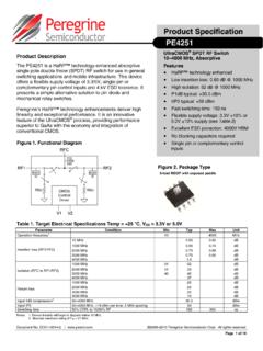
1 PE42823 Document Category: Product SpecificationUltraCMOS SPDT RF Switch, 700 MHz 6 GHz 2015 2017, Peregrine Semiconductor Corporation. All rights reserved. Headquarters: 9380 Carroll Park Drive, San Diego, CA, 92121 Product SpecificationDOC-67417-4 (05/2017) Excellent single-event peak power handling of51 dBm LTE Exceptional linearity performance across allfrequencies Input IP3: 70 dBm Input IP2: 105 dBm Extended operating temperature of +105 C TTL compatible control High ESD performance of kV HBM on RF pinsto ground Packaging 16-lead 3 3 mm QFNA pplications 4 wireless infrastructures Pre-5G/5G massive MIMO systems TDD-based RF transceiversProduct DescriptionThe PE42823 is a HaRP technology-enhanced 50 SPDT RF protection switch designed for use in high power and high performance wireless infrastructure applications such as macrocells supporting frequencies up to 6 switch features high linearity, which remains invariant across the full supply range.
2 The PE42823 also features exceptional isolation, fast switching time and is offered in a 16-lead 3 3 mm QFN package. In addition, no external blocking capacitors are required if 0 VDC is present on the RF PE42823 is manufactured on Peregrine s UltraCMOS process, a patented advanced form of silicon-on-insulator (SOI) s HaRP technology enhancements deliver high linearity and excellent harmonics performance. It is an innovative feature of the UltraCMOS process, offering the performance of GaAs with the economy and integration of conventional 1 PE42823 Functional DiagramANT (RFC)RX(RF2)TX(RF1)R((RCTRLVDDCMOS Control Driver and ESDPE42823 SPDT RF SwitchPage 2 DOC-67417-4 (05/2017) Maximum RatingsExceeding absolute maximum ratings listed in Table 1 may cause permanent damage. Operation should be restricted to the limits in Table 2.))
3 Operation between operating range maximum and absolute maximum for extended periods may reduce PrecautionsWhen handling this UltraCMOS device, observe the same precautions as with any other ESD-sensitive devices. Although this device contains circuitry to protect it from damage due to ESD, precautions should be taken to avoid exceeding the rating specified in Table ImmunityUnlike conventional CMOS devices, UltraCMOS devices are immune to 1 Absolute Maximum Ratings for PE42823 ParameterConditionMinTypMaxUnitPower supply voltage on CTRL input on LS input temperature range 65150 CInput power, avg:700 1800 MHzTx mode, 10-second duration,8dB PAR LTE signalNo power applied to off-terminated port. No hot 3800 6000 MHz42dBmESD voltage HBM:RF pins to GNDH uman body model (MIL-STD 883 Method 3015).4500 VAll pins4000 VESD voltage CDM, all pinsCharged device model (JEDEC JESD22-C101).
4 1250 VDOC-67417-4 (05/2017)Page RF SwitchRecommended Operating ConditionsTable 2 lists the recommending operating conditions for the PE42823 . Devices should not be operated outside the recommended operating conditions listed 2 Recommended Operating Conditions for PE42823 ParameterMinTypMaxUnitPower supply supply current120200 AControl voltage voltage low current10 AOperating temperature range 40+25+105 CPE42823 SPDT RF SwitchPage 4 DOC-67417-4 (05/2017) SpecificationsTable 3 provides the PE42823 key electrical specifications @ +25 C, VDD = , unless otherwise specified. Table 3 PE42823 Electrical SpecificationsParameterPathConditionMinT ypMaxUnitOperational frequency7006000 MHzInsertion lossANT RX700 MHz2100 MHz2700 MHz3800 MHz6000 TX700 MHz2100 MHz2700 MHz3800 MHz6000 RX700 MHz2100 MHz2700 MHz3800 MHz6000 MHz58464237305947433831dBdBdBdBdBANT TX700 MHz2100 MHz2700 MHz3800 MHz6000 MHz47363328224837342923dBdBdBdBdBReturn lossANT RX700 2700 MHz2701 3800 MHz3800 6000 MHz241712dBdBdBANT TX700 2700 MHz2701 3800 MHz3800 6000 MHz262628dBdBdBInput 1dB compressionANT TX700 3800 MHz3801 6000 MHz4643dBmdBmInput IP3 ANT RX70dBmInput IP2 ANT RX105dBmMax RF input powerTx modeContinuous Wave, 40 C to 105 mode Continuous Wave, 40 C to 105 C33dBmSettling time50% CTRL to dB final value ( 40 C to +105 C) Rising Edge2 sSettling time50% CTRL to dB final value ( 40 C to +105 C)
5 Falling sSwitching timeANT RX50% CTRL to 90% or 10% of final sANT TX50% CTRL to 90% or 10% of final sDOC-67417-4 (05/2017)Page RF SwitchControl LogicTable 4 provides the control logic truth table for the InformationThis section provides pinout information for the PE42823 . Figure 2 shows the pin map of this device for the available package. Table 5 provides a description for each pin. Table 4 Truth Table for PE42823 CTRLANT TXANT RX0 OFFON1 ONOFFF igure 2 Pin Configuration (Top View)ExposedGround PadGNDTXGNDGNDGNDGNDANTGNDGNDRXGNDGNDVDD NCCTRLGND13241210119576816141513 Pin 1 DotMarkingTable 5 Pin Descriptions for PE42823 Pin NameDescription1, 3, 4, 5, 6, 8, 9, 10, 12, RF RF RF control logic NC 16 VDDP ositive power supply : *RF pins 2, 7 and 11 must be at 0 VDC. The RF pins do not require DC blocking capacitors for proper operation if the 0 VDC require-ment is RF SwitchPage 6 DOC-67417-4 (05/2017) 3 Insertion Loss vs Temp (RF1)Figure 4 Insertion Loss vs VDD (RF1)Figure 5 Insertion Loss vs Temp (RF2) on Loss (dB)Frequency (GHz)-40 C+25 C+85 C+105 C on Loss (dB)Frequency (GHz) on Loss (dB)Frequency (GHz)-40 C+25 C+85 C+105 CFigure 6 Insertion Loss vs VDD (RF2)Figure 7 RFC Port Return Loss vs Temp (RF1)Figure 8 RFC Port Return Loss vs Temp (RF2) on Loss (dB)Frequency (GHz) Loss (dB)Frequency (GHz)-40 C+25 C+85 C+105 C rn Loss (dB)Frequency (GHz)-40 C+25 C+85 C+105 CDOC-67417-4 (05/2017)Page RF SwitchFigure 9 Isolation vs Temp (RF1-RF2, RF1 Active)
6 Figure 10 Isolation vs Temp (RF2-RF1, RF2 Active) (dB)Frequency (GHz)-40 C+25 C+85 C+105 C (dB)Frequency (GHz)-40 C+25 C+85 C+105 CFigure 11 Isolation vs Temp (RFC-RF1, RF2 Active) (dB)Frequency (GHz)-40 C+25 C+85 C+105 CPE42823 SPDT RF SwitchPage 8 DOC-67417-4 (05/2017) BoardFigure 12 Evaluation Kit Layout for PE42823 PRT-30188-02R1R2R3R7C1R5C2C3R4R6C4J4 DGNDVSS/GNDVDDGNDLSU1 RFCTHRUJ5J6J2RF2J13X3 16L QFN SPDTRF1J3 DOC-67417-4 (05/2017)Page RF SwitchPackaging InformationThis section provides packaging data including the moisture sensitivity level, package drawing, package marking and tape-and-reel Sensitivity LevelThe moisture sensitivity level rating for the PE42823 in the 16-lead 3 3 mm QFN package is DrawingTop-Marking SpecificationFigure 13 Package Mechanical Drawing for 16-lead 3 3 mm QFNF igure 14 Package Marking Specifications for PE42823 TOP VIEWBOTTOM VIEWSIDE VIEWRECOMMENDED LAND (2X) (2X) FEATURESPIN #1 (x16) (x16) (x12) (x16) (x16) (x12) =WW =ZZZZZZ =Pin 1 indicatorLast two digits of assembly yearAssembly work weekAssembly lot code (maximum six characters)42823 YYWWZZZZZZPE42823 SPDT RF SwitchPage 10 DOC-67417-4 (05/2017)
7 And Reel SpecificationFigure 15 Tape and Reel Specifications for 16-lead 3 3 mm QFNTK0A0B0P0P1D1 ASection A-AADirection of FeedD0EW0P2see note 3seenote 1 Fsee note + Orientation in TapePin 1 Notes:1. 10 Sprocket hole pitch cumulative tolerance Camber in compliance with EIA 4813. Pocket position relative to sprocket hole measuredas true position of pocket, not pocket hole PE42823 SPDT RF SwitchProduct (05/2017)Document CategoriesAdvance InformationThe product is in a formative or design stage. The datasheet contains design target specifications for product development. Specifications andfeatures may change in any manner without SpecificationThe datasheet contains preliminary data. Additional data may be added at a later date. Peregrine reserves the right to change specifications at anytime without notice in order to supply the best possible SpecificationThe datasheet contains final data.
8 In the event Peregrine decides to change the specifications, Peregrine will notify customers of the intendedchanges by issuing a CNF (Customer Notification Form). Sales ContactFor additional information, contact Sales at information in this document is believed to be reliable. However, Peregrine assumes no liability for the use of this information. Use shall beentirely at the user s own risk. No patent rights or licenses to any circuits described in this document are implied or granted to any third s products are not designed or intended for use in devices or systems intended for surgical implant, or in other applications intended tosupport or sustain life, or in any application in which the failure of the Peregrine product could create a situation in which personal injury or deathmight occur.
9 Peregrine assumes no liability for damages, including consequential or incidental damages, arising out of the use of its products insuch StatementPeregrine products are protected under one or more of the following patents: and Trademark 2015 2017, Peregrine Semiconductor Corporation. All rights reserved. The Peregrine name, logo, UTSi and UltraCMOS are registered trade-marks and HaRP, MultiSwitch and DuNE are trademarks of Peregrine Semiconductor InformationTable 6 lists the available ordering codes for the PE42823 as well as available shipping 6 Order Codes for PE42823 Order CodesDescriptionPackagingShipping MethodPE42823A XPE42823 SPDT RF switch16-lead 3 3 mm QFN500 units/T&REK42823 01PE42823 Evaluation kitEvaluation kit1/Box