Transcription of Features HaRP™-Technology-Enhanced Eliminates …
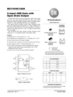
1 Document No. 70-0246-03 Page 1 of 9 2008 Peregrine Semiconductor Corp. All rights reserved. RF1RF2 CTRLLSRFC50 50 CMOSC ontrolDriverESDESD 16-lead 3x3 mm QFN Figure 2. Package Type The PE42552 RF Switch is designed for use in Test/ATE, cellular and other wireless applications. This broadband general purpose switch maintains excellent RF performance and linearity from DC through 7500 MHz. The PE42552 integrates on-board cmos control logic driven by a single-pin, low voltage cmos control input. It also has a logic select pin which enables changing the logic definition of the control pin. Additional Features include a novel user defined logic table, enabled by the on-board cmos circuitry. The PE42552 also exhibits outstanding isolation of 44 dB at 7500 MHz, fast settling time, and is offered in a tiny 3x3 mm QFN package. The PE42552 is manufactured on Peregrine s UltraCMOS process, a patented variation of silicon-on-insulator (SOI) technology on a sapphire substrate, offering the performance of GaAs with the economy and integration of conventional cmos .
2 Product Specification SPDT UltraCMOS RF Switch DC - 7500 MHz Product Description Figure 1. Functional Diagram PE42552 Features HaRP -Technology-Enhanced Eliminates Gate and Phase Lag No insertion loss or phase drift Fast settling time High linearity: 65 dBm IIP3 Low insertion loss: dB at GHz, dB at GHz, at GHz High isolation of 47 dB at GHz, 44 dB at GHz 1 dB compression point: + dBm typ. Logic Select pin to invert logic control High ESD: 1000 V HBM Absorptive switch design Standard 3x3 mm QFN package Table 1. Target Electrical Specifications Temp = 25 C, VDD = , VSS = 0V / Parameter Conditions Min Typical Max Units Operation Frequency MHz 9 kHz GHz Insertion Loss 9 KHz 3000 MHz 6000 MHz 7500 MHz dB dB dB dB Isolation RF1 to RF2 3000 MHz 6000 MHz 7500 MHz 45 32 25 47 34 28 dB dB dB Isolation RFC to RFX 3000 MHz 6000 MHz 7500 MHz 44 49 37 47 55 44 dB dB dB Return Loss 3000 MHz 6000 MHz 7500 MHz 20 25 15 dB dB dB Settling Time 50% CTRL to dB final value (-40 to +85 C) Rising Edge 50% CTRL to dB final value (-40 to +85 C) Falling Edge 9 15 11 45 Switching Time 50% CTRL to 90% or 10% of final value (-40 to +85 C) 5 7 s Input 1 dB Compression 800 MHz 7500 MHz 32 34 dBm dBm Input IP3 7500 MHz 65 dBm Input IP2 7500 MHz 100 dBm s s REPLACE WITH PE42553 OBSOLETELogo updated under non-rev change.
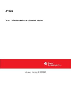
3 Peregrine products are protected under one or more of the following Patents: Specification PE42552 Page 2 of 9 2008 Peregrine Semiconductor Corp. All rights reserved. Document No. 70-0246-03 UltraCMOS RFIC Solutions Table 2. Pin Descriptions Table 4. Absolute Maximum Ratings Electrostatic Discharge (ESD) Precautions When handling this UltraCMOS device, observe the same precautions that you would use with other ESD-sensitive devices. Although this device contains circuitry to protect it from damage due to ESD, precautions should be taken to avoid exceeding the rating specified. Latch-Up Avoidance Unlike conventional cmos devices, UltraCMOS devices are immune to latch-up. Figure 3. Pin Configuration (Top View) Pin No. Pin Name Description 2 RF1 RF Port 1 1, 3, 4, 5, 6, 8, 9, 10, 12 GND Ground 7 RFC RF Common 11 RF2 RF Port 2 13 VSS Negative supply voltage or GND connection (Note 1) 14 CTRL cmos level: 15 LS Logic Select - Used to determine the definition for the CTRL pin (see Table 5) 16 VDD Nominal V supply connection Table 5.
4 Control Logic Truth Table GNDGNDRFCGNDGNDRF1 GNDGNDGNDGNDRF2 GNDVssCTRLLSVdd11615141312111095678234 Exceeding absolute maximum ratings may cause permanent damage. Operation should be restricted to the limits in the Operating Ranges table. Operation between operating range maximum and absolute maximum for extended periods may reduce reliability. Symbol Parameter/Conditions Min Max Units VDD Power supply voltage V VI Voltage on any input except for CTRL and LS inputs VDD+ V VCTRL Voltage on CTRL input V VLS Voltage on LS input V TST Storage temperature range -65 150 C PIN Input Power: 9 kHz 1 MHz 1 MHz GHz fig. 4,5 30 dBm dBm VESD ESD voltage (HBM)1 ESD voltage (Machine Model) 1000 100 V V Table 3. Operating Ranges Parameter Min Typ Max Units VDD Positive Power Supply Voltage V VSS Negative Power Supply Voltage (external power supply used) V IDD Power Supply Current (VSS = 0V, Temp = +85 C) 15 120 A Control Voltage High V Control Voltage Low V RF Power In1(PIN): 9 kHz 1 MHz 1 MHz GHz fig.
5 4,5 30 dBm dBm VSS Negative Power Supply Voltage (internal power supply used) V ISS Negative Supply (VSS = -VDD, Temp = 25 C) -10 -40 A TOP Operating temperature range -40 25 85 C Note: 1. Please consult low frequency graphs on page 3 for recommended operating power level. Note: 1. Human Body Model (HBM, MIL_STD 883 Method ) Moisture Sensitivity Level The Moisture Sensitivity Level rating for the PE42552 in the 16-lead 3x3mm QFN package is MSL1. Logic Select (LS) The Logic Select feature is used to determine the definition for the CTRL pin. Note: 1. Use VSS (pin 13, VSS = -VDD) to bypass and disable internal negative voltage generator. Connect VSS (pin 13) to GND (VSS = 0V) to enable internal negative voltage generator. Switching Frequency The PE42552 has a maximum 25 kHz switching rate when the internal negative voltage generator is used (pin 13=GND). The rate at which the PE42552 can be switched is only limited to the switching time (Table 1) if an external negative supply is provided at (pin13=VSS).
6 LS CTRL RFC-RF1 RFC-RF2 0 0 off on 0 1 on off 1 0 on off 1 1 off on Spurious Performance The typical spurious performance of the PE42552 is -116 dBm when VSS=0V (pin 13 = GND). If further improvement is desired, the internal negative voltage generator can be disabled by setting VSS = -VDD. REPLACE WITH PE42553 OBSOLETELogo updated under non-rev change. Peregrine products are protected under one or more of the following Patents: Specification PE42552 Page 3 of 9 Document No. 70-0246-03 2008 Peregrine Semiconductor Corp. All rights reserved. (V)Input Power (dBm)Upper Power Limit0510152025301101001000 Freq (kHz)Operating Power Offset (dB)Figure 5 shows how the power limit in Figure 4 will increase with frequency.
7 As the frequency increases, the contours and Maximum Power Limit Curve will increase with the increase in power handling shown on the curve. Figure 4. Maximum Operating Power Limit vs. Vdd and Input Power @ 9 KHz Figure 5. Operating Power Offset vs. Frequency (Normalized to 9kHz) Figure 4 provides guidelines of how to adjust the Vdd and input Power to the 42552 device. The upper limit curve represents the maximum Input Power vs Vdd recommended for this part. To allow for sustained operation under any load VSWR condition, max power should be kept 6dB lower than max power in 50 Ohm. Power Handling Examples Example 1: Maximum power handling at 100kHz, Z=50 ohms, VSWR 1:1, and Vdd=3V The power handling offset for 100kHz from Fig. 5 is 10dB The max power handling at Vdd = 3V is from Fig. 4 Derate power under mismatch conditions Total maximum power handling for this example is 10dB + = Low Frequency Power Handling: ZL = 50 REPLACE WITH PE42553 OBSOLETELogo updated under non-rev change.
8 Peregrine products are protected under one or more of the following Patents: Specification PE42552 Page 4 of 9 2008 Peregrine Semiconductor Corp. All rights reserved. Document No. 70-0246-03 UltraCMOS RFIC Solutions [GHz]Insertion Loss [-dB] [GHz] Insertion Loss [-dB]RF1 PathRF2 Path-100-90-80-70-60-50-40-30-20-1000123 456789 Frequency [GHz]Isolation [-dB]+25deg C+85deg C-40deg C-100-90-80-70-60-50-40-30-20-1000123456 789 Frequency [GHz]Isolation [-dB] V-100-90-80-70-60-50-40-30-20-1000123456 789 Frequency [GHz]Isolation [-dB]+25deg C+85deg C-40deg [GHz]Insertion Loss [-dB]+25deg C+85deg C-40deg CFigure 9. Isolation: Active Port to Isolated Port @ V Figure 8. Insertion Loss: RFX @ 25 C Figure 6. Nominal Insertion Loss: RF1, RF2 Figure 7. Insertion Loss: RFX @ V Performance Plots: Temperature = 25 C, VDD = V unless otherwise indicated Figure 10. Isolation: Active Port to Isolated Port @ 25 C Figure 11. Isolation: RFC to Isolated Port @ V REPLACE WITH PE42553 OBSOLETELogo updated under non-rev change.
9 Peregrine products are protected under one or more of the following Patents: Specification PE42552 Page 5 of 9 Document No. 70-0246-03 2008 Peregrine Semiconductor Corp. All rights reserved. + + + + + + +10 Frequency [Hz]IIP3 [dBm] V-100-90-80-70-60-50-40-30-20-1000123456 789 Frequency [GHz]Isolation [-dB] V-35-30-25-20-15-10-500123456789 Frequency [GHz]Return Loss [-dB] V-30-25-20-15-10-500123456789 Frequency [GHz]Return Loss [-dB]+25deg C+85deg C-40deg CFigure 14. Return Loss at active port @ 25 C Figure 15. Return Loss at active port @ V Performance Plots: Temperature = 25 C, VDD = V unless otherwise indicated Figure 12. Isolation: RFC to Isolated Port @ 25 C Figure 13. IIP3: Third Order Distortion from 10kHz - REPLACE WITH PE42553 OBSOLETELogo updated under non-rev change. Peregrine products are protected under one or more of the following Patents: Specification PE42552 Page 6 of 9 2008 Peregrine Semiconductor Corp. All rights reserved.
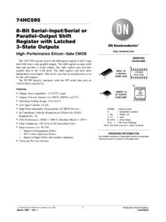
10 Document No. 70-0246-03 UltraCMOS RFIC Solutions Through LineL1 WAS INDUCTOR12J5142-0761-881/ 89112J1142-0761-881/ 89112J3142-0761-881/ 8911133557722446688101012121414131399111 1J4 HEADER 1412J2142-0761-881/ 891C122pFR1 DNIC222pFR2 DNIC322pF12J6142-0761-881/ 891R3 DNIC468pF9 GND10 GND11RF212 GND13 VSS14 CTRL15LS16VD D1 GND3 GND2RF 14 GND5 GND6 GND8 GND7 RFCU1 QFN50P3X3-16PR40 O H ML10 OHMLSRF2 CTRLVDDVSSRF 1 RFCE valuation Kit The SPDT switch EK Board was designed to ease customer evaluation of Peregrine s PE42552. The RF common port is connected through a 50 transmission line via the top SMA connector, J1. RF1, RF2, RF3 and RF4 are connected through 50 transmission lines via SMA connectors J3, J5, J2 and J4, respectively. A through 50 transmission is available via SMA connectors J6 and J7. This transmission line can be used to estimate the loss of the PCB over the environmental conditions being evaluated. The evaluation kit board is constructed of four metal layers.