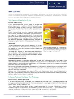
Transcription of Photolithography Overview for MEMS
1 Photolithography Overview Photolithography Overview for MEMSfor MEMS Knowledge ProbeKnowledge Probe Photolithography Overview PKPhotolithography Overview PK ActivityActivity TerminologyTerminology ActivityActivity Resist ThicknessResist Thickness Participant GuideParticipant Guide Southwest Center for Microsystems Education (SCME) University of New Mexico MEMS Fabrication Topic Photolithography Overview for Microsystems Knowledge Probe (Pre-Quiz) Shareable Content Object (SCO) This SCO is part of the Learning Module Photolithography Overview Target audiences: High School, Community College, University Support for this work was provided by the National Science Foundation's Advanced Technological Education (ATE) Program through Grant #DUE 0902411.
2 Any opinions, findings and conclusions or recommendations expressed in this material are those of the authors and creators, and do not necessarily reflect the views of the National Science Foundation. Copyright by the Southwest Center for Microsystems Education and The Regents of the University of New Mexico Southwest Center for Microsystems Education (SCME) 800 Bradbury Drive SE, Suite 235 Albuquerque, NM 87106-4346 Phone: 505-272-7150 Website: Southwest Center for Microsystems Education (SCME) Page 2 of 5 Fab_PrLith_KP00_PG_070112 Knowledge Probe Photolithography Photolithography Overview for Microsystems Knowledge Probe Participant Guide Objective of this Knowledge Probe (KP) The objective of this knowledge probe is to determine your current knowledge and understanding of the Photolithography processes used to fabricate micro-sized devices or MEMS.
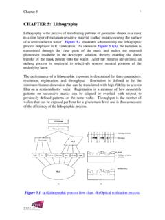
3 This KP should help you identify areas in which you need a better understanding and also assist the instructor in knowing what needs to be emphasized. Answer the following questions to the best of your knowledge. Don t worry if you don t know the answer. Select the answer that you think is correct. 1. Which of the following BEST describes the Photolithography process? a. The process step that transfers a pattern into an underlying layer or the substrate s bulk. b. The process step that defines and transfers a pattern into a resist layer on the wafer.
4 C. The process step that deposits a resist layer on the surface of the wafer. d. The process step that aligns the various layers of a microsystem device to each other. 2. What are the three (3) basic steps of the Photolithography process? a. Prime, expose, etch b. Prime, coat, expose c. Coat, mask, expose d. Coat, expose, develop 3. What are the elements of the image labels (A, B, C, D), respectively? a. Mask, photoresist, film to be etched, substrate b. Mask, layer to be etched, photoresist, substrate c. Mask, substrate, photoresist, metal layer d.
5 Mask, photoresist, primer, substrate Southwest Center for Microsystems Education (SCME) Page 3 of 5 Fab_PrLith_KP00_PG_070112 Knowledge Probe Photolithography 4. The photoresist film is applied in which of the following Photolithography steps. a. Prime b. Coat c. Mask d. Expose e. Develop 5. Prior to applying the photoresist layer, the surface of the wafer must be conditioned. Which of the following BEST describes the purpose of surface conditioning? a. Remove surface particles, dry the wafer s surface, create a hydrophilic surface b.
6 Dry the wafer, heat the wafer to better accept the resist, create a hydrophobic surface c. Clean and dry the wafer, create a hydrophobic and more adhesive surface d. Clean the surface, heat the wafer to better accept the resist and make it more adhesive 6. What is the chemical used in surface conditioning? a. HMDS (Hexamethyldixalizane) b. KOH (potassium hydroxide) c. Piranha (sulfuric acid and hydrogen peroxide) d. PMMA (polymethylmethacrylate) 7. There are two basic types of photoresist positive and negative. Which of the following statements is TRUE?
7 A. With positive resist, the exposed regions are dissolved during develop. b. With negative resist, the exposed regions are dissolved during develop. c. With positive resist, the exposed regions are hardened during develop. d. With negative resist, the exposed regions are hardened during develop. 8. Which of the following determine the final thickness of photoresist after the coat process? a. The viscosity of the resist and the amount of time that the wafer spins b. The spin speed after deposition of resist and the amount of time that the wafer spins c.
8 The amount of resist applied and the amount of time that the wafer spins d. The spin speed of the wafer after deposition of resist and the viscosity of the resist 9. During the coating of photoresist, the thickness of the photoresist _____ with an increase in spin speed. a. Increases exponentially b. Decrease exponentially c. Increase linearly d. Decreases linearly Southwest Center for Microsystems Education (SCME) Page 4 of 5 Fab_PrLith_KP00_PG_070112 Knowledge Probe Photolithography 10. What is the purpose of the softbake after resist application?
9 A. To remove residual solvent from the resist layer b. To correct minor uniformity problems with the resist c. To harden the resist for the expose process step d. To harden the resist for the etch process step 11. The expose step follows the _____ process step. a. Surface conditioning b. Coat c. Soft bake d. Hard bake 12. For the expose step, some Photolithography equipment, such as steppers, use a small quartz plate that contains the pattern for just a few die or fields on a wafer. This plate is called a _____. a.
10 Mask b. Reticle c. Partial mask d. Die plate 13. Which of the following two UV light sources are commonly used to expose the photoresist? a. Mercury Vapor Lamps and excimer lasers b. Mercury vapor lamps and compact fluorescent lamps c. CO2 Lasers and mercury vapor lamps d. CO2 Lasers and excimer lasers 14. After the coated wafer is placed into the Photolithography expose equipment, it is _____ prior to being exposed. a. Baked b. Cooled c. Aligned d. Coated 15. Which of the following could be the result of an underdeveloped resist layer?