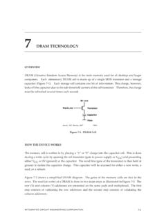
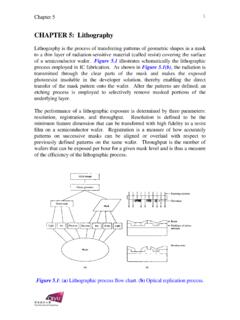
Transcription of Yield and Yield Management - Smithsonian Institution
1 3. Yield and Yield Management 3 Yield and Yield Management Clearly line Yield and defect density are two Yield improvement is the most critical goal of the most closely guarded secrets in the of all semiconductor operations as it reflects semiconductor industry. Line Yield refers to the amount of product that can be sold rela- the number of good wafers produced with- tive to the amount that is started. Yield is also out being scrapped, and in general, measures the single most important factor in overall the effectiveness of material handling, wafer processing costs. That is, incremental process control, and labor. Die Yield refers to increases in Yield (1 or 2 percent) signifi- the number of good dice that pass wafer cantly reduce manufacturing cost per wafer, probe testing from wafers that reach that or cost per square centimeter of silicon.
2 In the part of the process. It is intended to prevent fab, Yield is closely tied to equipment perfor- bad dice from being assembled into pack- mance (process capability), operator train- ages that are often extremely expensive and ing, overall organizational effectiveness, and measures the effectiveness of process control, fab design and construction. design margins, and particulate control. Figure 3-1 shows some typical numbers for a Continued device miniaturization in the few product types normalized to twenty semiconductor industry and the trend to masking layers, similar feature and die sizes, larger and larger die sizes means that partic- and the Murphy defect density model.
3 Ulate contamination has an ever increasing impact on yields. Today, over 80 percent of Best Average Worst Yield loss of VLSI chips manufactured in Product Metric Score Score Score volume can be attributed to random defects . Memory Line Yield The other main contributors to Yield loss Die Yield include design margin and process variation, CMOS Logic Line Yield followed by photolithography errors, and Die Yield material (wafer) defects (Figure 3-2). The dramatic decline in the contribution of MSI Line Yield people to particulate problems in the fab can Die Yield be attributed to better education and train- * 2Q mask layers, ~1m feature size, cm Source: UC Berkeley Study 22793.
4 Ing, adherence to clean room disciplines, and less direct contact by the people due to more Figure 3-1. Typical Line Yield and Die Yields use of automation. (Normalized*). INTEGRATED CIRCUIT ENGINEERING CORPORATION 3-1. Yield and Yield Management Yield . PROBE Yield PERCENT OF TOTAL PROBE. LOSS. PROBLEM Yield LOSS. (%). CONTAMINATION 40 80. DESIGN MARGIN 5 10. PROCESS VARIATION 3 6. PHOTOLITHOGRAPHY ERRORS 1 2. MATERIAL defects 1 2. TOTAL LOSS 50 100. PROBE Yield (100% - DIE LOSS) = 50%. Source: ICE 12056G. Figure 3-2. Typical 1996 Silicon Wafer IC Probe Yield Losses Random defects can be traced back to the of contamination in leading-edge fabs today tools, the people, the processes, the process is due to the processes and tools (Figure 3-3).
5 Chemicals and gases, or the cleanroom itself. However, for many existing fabs, cleanroom Over the years, cleanroom technology and contamination remains a significant, Yield - the purification of process materials has been limiting factor. improved so dramatically that the majority 100. 90. 80 Cleanroom 70 Processes Equipment 60. Percent People 50. 40. 30. 20. 10. 0. 1985 1990 1995 2000. Year Source: CleanRooms 19973A. Figure 3-3. Sources of Wafer-Level Contamination 3-2 INTEGRATED CIRCUIT ENGINEERING CORPORATION. Yield and Yield Management Contamination control involves the control problems that IC manufacturers face today. of particulates, transition metals, heavy The category of Class one clean room is inad- metals, organics, and any other undesirable equate in monitoring particles for some of contaminants that result from IC processing.
6 The future feature sizes due to the inaccura- Figure 3-4 shows some of the critical parame- cies of measuring particles that small. This ters that drive IC complexity over time, fact, along with the previously discussed including minimum device feature size, sources of particles today, may lead to the resist exposure wavelength, and maximum more pervasive use of mini-environments critical particle diameter also known as and robots as an alternative to the classical killer defect size. As shown, critical particle clean room designs. This has some major size is one-fifth the feature size at these small implications on the cost of tomorrow s fabs.
7 Geometries. Figure 3-5 illustrates one of the This will be addressed in a future section. DRAM Density 4M 16M 64M 256M 1G. Resolution ( m) Wavelength (nm) 436 365 365/248 248/193 193/157. Criticle Particle Diameter ( m). 1992 1993 1994 1995 1996 1997 1998 1999 2000 2001. Source: Sematech 19042. Figure 3-4. DRAM Evolution, Exposing Wavelength, and Critical Particle Diameter Class Limits Class Name m m m m Volume units Volume units Volume units Volume units SI English* (m3) (ft3) (m3) (ft3) (m3) (ft3) (m3) (ft3). M1 350 M 1 1,240 265 106 M2 3,500 757 309 100 M 10 12,400 350 2,650 1,060 353 M3 35,000 991 7,570 214 3,090 1,000 M 100 26,500 750 10,600 300 3,530 100.
8 M4 75,700 2,140 30,900 875 10,000 283. M 1,000 35,300 1,000. * For naming and describing the classes, SI names and units are preferred; however, English ( customary) units may be used. Source: Institute of Environmental Sciences 21409. Figure 3-5. Airborne Particulate Cleanliness Classes (FED-STD-209E). INTEGRATED CIRCUIT ENGINEERING CORPORATION 3-3. Yield and Yield Management In terms of the other major forms of conta- Another concern for Yield loss in the fab on mination, Figures 3-6 and 3-7[1] illustrate many device structures is ESD (electrostatic the types of contaminants that are common, discharge). Care must be exercised in the along with some of the more popular clean- design and construction of the facility and ing techniques used to remove them, equipment set to minimize the possibility of respectively.
9 Producing unwanted charges that can lead to device damage. The following common impurity elements from chemicals and processing can be deleterious to silicon devices: Heavy metals (most critical). Fe, Cu, Ni, Zn, Cr, Au, Hg, Ag Alkali metals (critical). Na, K, Li Light elements (less serious). Al, Mg, Ca, C, S, Cl, F. Source: Handbook of Wafer Cleaning Technology 21657. Figure 3-6. Impurity Elements Harmful to Silicon Wafers Processing Chemical Purpose or Solution Common Name Symbols Removal of: Ammonium hydroxide/ NH4OH/H2O2/H2O RCA-1, SC-1 (Standard Light organics, particles, hydrogen peroxide/ Clean-1), APM (ammo- and metals; protective water nia/peroxide mix), oxide regrowth Huang A.
10 Hydrochloric acid/ HCl/H2O2/H2O RCA-2, SC-2 (Standard Heavy metals, alkalis, hydrogen peroxide/ Clean-2), HPM (hydro- and metal hydroxides water chloric/peroxide mix), Huang B. Sulfuric acid/ H2SO4/H2O2 Piranha, SPM (sulfuric/ Heavy organics hydrogen peroxide peroxide mix), "Caros acid". Hydrofluoric acid/water HF/H2O HF, DHF (dilute HF) Silicon oxide Hydrofluoric acid/ HF/NH4F/H2O BOE (buffered oxide Silicon oxide ammonium fluoride/ etch), BHF (buffered hy- water drofluoric acid). Nitric acid HNO3 Organics and heavy metals Source: Handbook of Wafer Cleaning Technology 21666A. Figure 3-7. Partial List of Silicon Wafer Cleaning Solutions 3-4 INTEGRATED CIRCUIT ENGINEERING CORPORATION.