Example: confidence
Defect in crystals - Weizmann Institute of Science
Points defects Self-interstitial –A self-interstitial is an atom from the crystal that is crowded into an interstitial site, a small void space that under ordinary circumstances is not occupied. the formation of this defect is not highly probable, and it exists in
Tags:
Information
Domain:
Source:
Link to this page:
Documents from same domain

Nitrous oxide, compressed - Weizmann Institute of Science
www.weizmann.ac.ilNitrous oxide, compressed Safety Data Sheet P-4636 This SDS conforms to U.S. Code of Federal Regulations 29 CFR 1910.1200, Hazard Communication.

Safety Data Sheet - Weizmann Institute of Science
www.weizmann.ac.ilAldrich - 267961 Page1 of 7 SIGMA-ALDRICH sigma-aldrich.com SAFETY DATA SHEET according to Regulation (EC) No. 1907/2006 Version 5.0 Revision Date 29.10.2012 Print Date 19.04.2017 GENERIC EU MSDS - NO COUNTRY SPECIFIC DATA - NO OEL DATA

The Alkaloids - Weizmann Institute of Science
www.weizmann.ac.ilAlkaloids of Opium Poppy (Papaver) • Morphine named for Morpheus, the god of dreams in the Greek mythology • Friedrich Serturner isolated Morphine at 1806 and this gave rise to the study of alkaloids • In 1819, Carl Meissner (Halle) gave the name alkaloids after the plant al-qali from which soda was isolated (sodium

Loan Repayment Letter of Undertaking - Weizmann
www.weizmann.ac.ilfollowing month) and for _____ months until final repayment of said loan. 4. I am aware and give my expressed consent that the loan will be up for immediate repayment should I cease to be a student in the Institute for any reason or should I cease to receive payment from the Institute, for any other reason, unless a written

A Tutorial on Euler Angles and Quaternions
www.weizmann.ac.ilThe concept of coordinate transformations in three-dimensions is the same as in two dimensions, however, the mathematics are more complicated. Furthermore, many of us find it difficult to visualize explanations of three-dimensional motion when all we are shown is two-dimensional representations of three-dimensional objects.

Secondary Metabolites: Biochemistry and Role in Plants
www.weizmann.ac.ilCo-evolution in plant SMs - natural enemy - Canavanine is toxic due to its incorporation into proteins that rise to functionally aberrant polypeptides - The tRNA- Arginine in insects uses also Canavanine - The insect mutated its tRNA and will not incorporate canavanine instead of …

Tutorial 1 - Graphene
www.weizmann.ac.ilRemember that a honeycomb lattice is actually an hexagonal lattice with a basis of two ions in each unit cell. If ais the distance between nearest neighbors, the primitive lattice vectors can be chosen to be ... This is just the 2D massless Dirac Hamiltonian, which describes free relativistic electrons, where the speed of light has been ...
Related documents
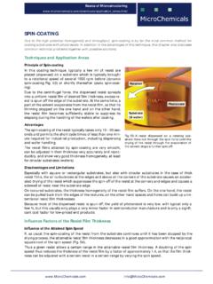
Spin-coating of Photoresists - MicroChemicals
microchemicals.comthe resist fi lm becomes suffi ciently stable to suppress its elapsing during the handling of the wafers after coating. Advantages The spin-coating of the resist typically takes only 10 - 20 sec- ... Inhomogeneous Resist Film Thickness and Resist Defects Textured Substrates.

Photolithography Overview for MEMS
nanoscale.unl.eduThe amount of resist applied and the amount of time that the wafer spins d. The spin speed of the wafer after deposition of resist and the viscosity of the resist 9. During the coating of photoresist, the thickness of the photoresist _____ with an increase in spin speed. ... Defects (particles, scratches, etc.) 17. The final test on a micro ...

An Overview of Forging Processes with Their Defects - IJSRP
www.ijsrp.orgdefects that are lightly to come if a proper care is not taken in forging process design. Defects can be defined as the ... to resist abrasion wear due to scales present on work piece. Selection of proper die material depends on: Die size, Composition and properties of …

WARNING: This product contains chemicals known to the ...
www.crimsontrace.comLaser sights require minimal attention and are designed to resist most common firearm chemicals and lubricants, however, excessive exposure to these chemicals can be detrimental. ... warrants that this product will be free from defects in materials and workmanship for a period of three years from the original retail purchase. CTC will repair or ...
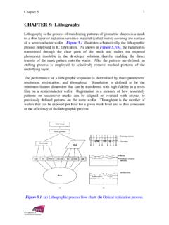
CHAPTER 5: Lithography - City University of Hong Kong
www.cityu.edu.hkcause defects in the devices. As illustrated in Figure 5.2, airborne particles adhering to the surface of a photomask behave as opaque patterns that can be ... patterns onto a resist-coated wafer many centimeters away from the mask. The small image area is scanned or stepped over the wafer to cover the entire surface.
Lecture 25: Lithography
nptel.ac.inexcess resist is removed, and there is a uniform lm over the entire surface. The right amount of resist should be added, so that coverage is uniform but not excessive, as shown in gure 10. The nal resist thickness depends on the amount of resist, spin speed, viscosity, surface tension, and drying char-acteristics (solvent dependent).

How to Build a Printed Circuit Board
www.4pcb.comResist Strip The developed dry film resist is now removed from the panel. The tin plating is not affected. Any holes that were covered with resist are now open and will be non-plated. This is the first step in the common phrase “strip-etch-strip”or …

Yield and Yield Management - Smithsonian Institution
smithsonianchips.si.eduvolume can be attributed to random defects. The other main contributors to yield loss include design margin and process variation, followed by photolithography errors, and material (wafer) defects (Figure 3-2). The dramatic decline in the contribution of people to particulate problems in the fab can be attributed to better education and train-
Temperature Dependence of Semiconductor Conductivity
www.iiserkol.ac.inImpurity scattering is caused by crystal defects such as ionized impurities. At lower temperatures, carriers move more slowly, so there is more time for them to interact with charged impurities. As a result, as the temperature decreases, impurity scattering increases, and the mobility decreases.