Search results with tag "Lithography"

Optics for EUV Lithography
www.euvlitho.comOptics for EUV Lithography have evolved over three decades to a level where excellent imaging is demonstrated. Right now, the Starlith ® 3400 Optics extends EUV Lithography to 13nm single-shot resolution with high productivity for serial production. High-NA EUV Lithography enables further shrink for the

Roll to Roll (R2R) Processing Technology Assessment
www.energy.gov172 Imprint or Soft Lithography – In soft lithography (e.g. self-aligned imprint lithography (SAIL)), 173 multiple mask levels are imprinted as a single three dimensional (3-D) structure as shown in 174 Figure 4. The photopolymer layer is heated above its glass transition temperature to allow it to 175 flow into the crevices of the stamp.

High-NA EUV Lithography Exposure Tool
conference-indico.kek.jpPublic 22 January 2021, EUV-FEL Workshop, Japan / Cloud High-NA EUV Lithography Exposure Tool For EUV roadmap extension Carl Zeiss SMT GmbH, Oberkochen, Germany Paul Graeupner ASML Veldhoven, The Netherlands Jan van Schoot, Jos Benschop, Sjoerd Lok, Eelco van Setten, Ruben Maas, Kars Troost, Jo Finders .

The Work of Art in the Age of Mechanical Reproduction
web.mit.eduLithography enabled graphic art to illustrate everyday life, and it began to keep pace with printing. But only a few decades after its invention, lithography was surpassed by photography. For the first time in the process of pictorial reproduction, photography freed the hand of the most important artistic

Nanoscale silicon field effect transistors fabricated using ...
www.princeton.edunanoimprint lithography. With this lithographic technique and dry etching, we have patterned a variety of nanoscale transistor features in silicon, including 100 nm wire channels, 250-nm-diam quantum dots, and ring structures with 100 nm ring width, over a 232 cm lithography field with good uniformity.

Patterning of light-extraction nanostructures on sapphire ...
www.princeton.edunanoimprint lithography. The SiO 2 mask patterning has five key steps (figures 1(a)–(d)): (1) deposition of a 350nm thick SiO 2 layer on sapphire by plasma-enhanced chemical vapor deposition at 250°C, using a mixture of silane (SiH 4)and nitrous oxide (N 2O); (2) UV nanoimprint lithography of nanoholes with 200nm pitch and 125nm diameter ...

Photoresist Strip Challenges for Advanced Lithography at ...
www.axcelis.comPhotoresist Strip Challenges for Advanced Lithography at 20nm Technology Node and Beyond Written by: Ivan L. Berry III, Carlo Waldfried, Dwight Roh, Shijian Luo, David Mattson, James DeLuca, and Orlando Escorcia (Axcelis Technologies)

SPECIAL REPORTS 半導体リソグラフィ技術の動向と東芝の …
www.global.toshibaLithography technology, which transfers a device circuit pattern printed on a mask to a silicon wafer using an exposure tool, plays a critical role in the semiconductor device manufacturing process and is continuously evolving to realize the shrinkage of semiconductor devices. As optical

Introducing Intel Foundry Services
newsroom.intel.comMar 23, 2021 · drive the next generation of lithography innovation to deliver a new era of Moore's Law.” Peter Wennink, CEO and president, ASML “Cadence and Intel have forged a deep partnership to enable the design ecosystem to use Intel's leading-edge process technologies. With Intel's announcement today, we are excited to
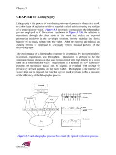
CHAPTER 5: Lithography - City University of Hong Kong
www.cityu.edu.hkcause defects in the devices. As illustrated in Figure 5.2, airborne particles adhering to the surface of a photomask behave as opaque patterns that can be ... patterns onto a resist-coated wafer many centimeters away from the mask. The small image area is scanned or stepped over the wafer to cover the entire surface.

The Chip Scale Package (CSP) - Intel
www.intel.comlithography process reductions (die shrinks), so does the package. At a certain point, the associated ball pitch will get smaller as well, in order to accommodate the smaller size of the die. This eventually leads to ball pitches as small as .5mm and below. Currently the majority of µbga packages are in .75mm pitch.

Fabrication and Manufacturing (Basics)
people.ee.duke.edu– Photo-light lithography, n. process of printing from a plane surface on which image to be printed is ink-receptive and the blank area is ink-repellant • Cover the wafer with a light-sensitive, organic material called photoresist • Expose to light with the proper pattern (mask) • Patterns left by photoresist can be used to control where

MINISTRY OF LABOUR AND EMPLOYMENT
labour.gov.in5*[(ca)] "competent person", in relation to any provision of ... lithography, photogravure or other similar process or book binding;] 3*[or] ... Chapter IX or section 108, section 109 or section 110, in relation to- (a) the workers employed directly by him, or

Fabrication of antiscatter grids and collimators for X-ray ...
www.creatvmicrotech.comTECHNICAL PAPER Fabrication of antiscatter grids and collimators for X-ray and gamma-ray imaging by lithography and electroforming Olga V. Makarova Æ Guohua Yang Æ

Nanoimprint lithography - Welcome to Nanonex
www.nanonex.comTypically, the intrusion of the mold is from 40 to 200 nm and the aspect ratio for the smallest mold features is 3:1. The thickness of the resist is from 50 to 250 nm.

Lithography Using ASML Stepper - diyhpl.us
diyhpl.usLithography Using ASML Stepper Page 4 INTRODUCTION Overlay (alignment) is as important as resolution in lithography. Modern CMOS integrated circuits have ~ 30 layers to be aligned. The RIT SUB-CMOS processes use up to 15 layers. Alignment marks are placed on the wafer at the beginning of the process
Similar queries
Lithography, High-NA EUV Lithography Exposure Tool, Public, ASML, The Age of Mechanical Reproduction, Nanoimprint lithography, Photoresist Strip Challenges for Advanced Lithography, SPECIAL REPORTS, Foundry, CHAPTER 5: Lithography, Defects, Resist, Intel, Chapter, Antiscatter grids and collimators for X-ray, Imaging by lithography and electroforming, Mold