Example: bankruptcy
Fabrication and Manufacturing (Basics)
– Photo-light lithography, n. process of printing from a plane surface on which image to be printed is ink-receptive and the blank area is ink-repellant • Cover the wafer with a light-sensitive, organic material called photoresist • Expose to light with the proper pattern (mask) • Patterns left by photoresist can be used to control where
Tags:
Information
Domain:
Source:
Link to this page:
Documents from same domain
ISSN 1751-8725 Wide angle impedance matching …
people.ee.duke.eduknown as metamaterials, in the wide angle impedance matching (WAIM) of waveguide-fed phased-array antennas. The authors propose that the anisotropic properties of a metamaterial layer, when designed

Boundary Scan Tutorial - All Faculty
people.ee.duke.eduBoundary Scan Tutorial 1 Boundary Scan Tutorial ... revised in 1993 and 1994, and most recently in 2001. You can obtain a copy of ... referred to as “1149.1a-1993,” contained many clarifications, corrections, and minor enhancements. Two new instructions were introduced in 1149.1a and these are described in this tutorial.
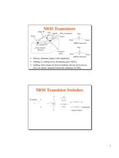
MOS Transistors - Faculty
people.ee.duke.eduD Flip-flop Operation 40 Race Condition • Back-to-back flops can malfunction from clock skew – Second flip-flop fires late – Sees first flip-flop change and captures its result ... Chip Cells Polygons Transistors Gates Processor Boolean equations Differential equations
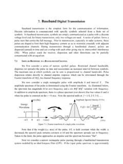
7. Baseband Digital Transmission
people.ee.duke.eduAdditionally, an ideal filter must have an impulse response that extends to infinite time before and after the pulse peak and, if the filter is to be causal (output response occurs after the input is applied), the peak output would occur an infinite time after the input. This would

MOS Transistor Theory
people.ee.duke.eduMOS Transistor Theory • So far, we have viewed a MOS transistor as an ideal switch (digital operation) – Reality: less than ideal. EE 261 James Morizio 2. EE 261 James Morizio 3 Introduction • So far, we have treated transistors as ideal switches • An ON transistor passes a finite amount of current – Depends on terminal voltages ...
Dynamic Combinational Circuits
people.ee.duke.edu– Transistors are leaky (I OFF „ 0) – Dynamic value will leak away over time – Formerly miliseconds, now nanoseconds! • Use keeper to hold dynamic node – Must be weak enough not to fight evaluation A f H 2 2 1 k X Y weak keeper. James Morizio 15 Charge Sharing (redistribution) Mp M e VDD Out A

8-bit Arithmetic Logic Unit Design Report
people.ee.duke.eduALU (Arithmetic Logic Unit) A critical component of the microprocessor, the core component of central processing unit. ALU comprises the combinational logic that implements logic operations such as AND and OR, and arithmetic operations such as …

The group lasso for logistic regression
people.ee.duke.edulogistic regression models and proposed a gradient descent algorithm to solve the correspond-ing constrained problem. We present methods which allow us to work directly on the penalized problem and whose convergence property does not depend on …
Related documents

Optics for EUV Lithography
www.euvlitho.comOptics for EUV Lithography have evolved over three decades to a level where excellent imaging is demonstrated. Right now, the Starlith ® 3400 Optics extends EUV Lithography to 13nm single-shot resolution with high productivity for serial production. High-NA EUV Lithography enables further shrink for the

Roll to Roll (R2R) Processing Technology Assessment
www.energy.gov172 Imprint or Soft Lithography – In soft lithography (e.g. self-aligned imprint lithography (SAIL)), 173 multiple mask levels are imprinted as a single three dimensional (3-D) structure as shown in 174 Figure 4. The photopolymer layer is heated above its glass transition temperature to allow it to 175 flow into the crevices of the stamp.
The Work of Art in the Age of Mechanical Reproduction
web.mit.eduLithography enabled graphic art to illustrate everyday life, and it began to keep pace with printing. But only a few decades after its invention, lithography was surpassed by photography. For the first time in the process of pictorial reproduction, photography freed the hand of the most important artistic

The Chip Scale Package (CSP) - Intel
www.intel.comlithography process reductions (die shrinks), so does the package. At a certain point, the associated ball pitch will get smaller as well, in order to accommodate the smaller size of the die. This eventually leads to ball pitches as small as .5mm and below. Currently the majority of µbga packages are in .75mm pitch.

Introducing Intel Foundry Services
newsroom.intel.comMar 23, 2021 · drive the next generation of lithography innovation to deliver a new era of Moore's Law.” Peter Wennink, CEO and president, ASML “Cadence and Intel have forged a deep partnership to enable the design ecosystem to use Intel's leading-edge process technologies. With Intel's announcement today, we are excited to

SPECIAL REPORTS 半導体リソグラフィ技術の動向と東芝の …
www.global.toshibaLithography technology, which transfers a device circuit pattern printed on a mask to a silicon wafer using an exposure tool, plays a critical role in the semiconductor device manufacturing process and is continuously evolving to realize the shrinkage of semiconductor devices. As optical

Lithography Using ASML Stepper - diyhpl.us
diyhpl.usLithography Using ASML Stepper Page 4 INTRODUCTION Overlay (alignment) is as important as resolution in lithography. Modern CMOS integrated circuits have ~ 30 layers to be aligned. The RIT SUB-CMOS processes use up to 15 layers. Alignment marks are placed on the wafer at the beginning of the process