Transcription of Post Exposure Bake (PEB) - MicroChemicals
1 Chapter01 MicroChemicals Fundamentals of of Exposure BAKEThe term "post Exposure bake" (PEB) refers to a baking step of the resist fi lm which follows the Exposure . Since the resist fi lm is not yet developed, that is to say closed, the PEB can also be applied without diffi culty above the softening temperature of the photoresist. There are several completely diff erent possible reasons for a PEB that are explained in this Amplifi ed Positive ResistsMechanismWhile with "normal" positive resists, the photoreaction with the Exposure is completed, chemically ampli-fi ed photoresists need a subsequent baking step.
2 This Post Exposure Bake (PEB) completes the photore-action initiated during Exposure . "Chemical amplifi cation" takes place when the reaction products formed during the Exposure in the resist fi lm works catalytically, which also allows thick resist fi lms to be exposed with comparable low doses and yet be developed at a high ConditionsWithout PEB, the resist fi lms would not develop or could only be developed at an extremely low rate. The necessary times and temperatures do not depend on the resist fi lm thickness but on the photoresist used and are typically 100-110 C for a few minutes.
3 Among the AZ positive resists we distribute (status: 2017), only the AZ 40 XT and IPS 6050 are chemically amplifi ed and therefore require a Reversal Resists and Cross-linking Negative ResistsMechanismImage reversal resists such as the AZ 5214E or TI 35 E/ESX require a PEB, usually referred to as an image reversal step, to invert the already exposed areas, thus later rendering them insoluble in the developer for processing in the negative resists, such as the AZ nLOF 2000 negative resist series or the AZ 15 nXT, require a PEB in order to carry out the cross-linking, which is initiated during Exposure rendering the exposed structures insoluble in the ConditionsThe necessary times and temperatures do not depend on the resist fi lm thickness, but on the photoresist used and are typically 110-130 C for a few higher the temperature of this baking step is chosen for image reversal resists, the more stable these structures are during development, however the more the photosensitivity suff ers and the later develop-ment rate of the previously unexposed, later fl ood-exposed areas of the hotter the PEB is carried out on negative resists.
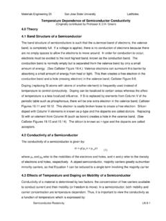
4 The higher the degree of cross-linking, and the more stable these structures are later in the developer. However, as the PEB temperature increases, the ther-mal cross-linking of the not yet exposed resist areas increases, which can therefore be more diffi cult to all negative resists require a PEB: In the case of the AZ 125 nXT, cross-linking takes place immediately during the Exposure at room Resists on highly Refl ective SubstratesMechanismApplying monochromatic Exposure of resists on refl ective substrates, an intensity distribution forms in-terference-caused in the resist fi lm which is Sin2-modulated in the incidental light direction.
5 This light pat-tern transfers to a spatially inhomogeneous development rate through the concentration distribution of the formed product of the photoreaction and thus into irregularly developed resist baking step after Exposure contributes to smoothing of the concentration profi le of the product of the photoreaction via its diff usion (Fig. 95) whereby the subsequently developed resist structures have steep-er and smoother sidewalls. Chapter01 MicroChemicals Fundamentals of of ConditionsThe necessary times and temperatures do not depend on the resist fi lm thickness, but on the photoresist used and are typically 110-120 C for a few minutes.
6 Details can be found in the corresponding technical data maskResist fi lmFig. 95: The monochromatic Exposure of a resist fi lm on a highly refl ective substrate results in a sin2-modulated intensity distribution (increasing from blue via red to white) of the product of the photoreaction (far left) in the direction of the inci-dental light. A baking step carried out under suitable conditions smoothens this concentration pattern by diff usion (from the left to the right the chronological sequence of a numerical modelling).SubstrateSlit Our Photoresists: Application Areas and Compatibilities Recommended Applications 1 Resist Family Photoresists Resist Film Thickness 2 Recommended Developers 3 Recommended Re-movers 4 1 In general, almost all resists can be used for almost any application.
7 However, the special properties of each resist family makes them specially suited for certain fields of application. 2 Resist film thickness achievable and processable with standard equipment under standard conditions. Some resists can be diluted for lower film thicknesses; with additional effort also thicker resist films can be achieved and processed. 3 Metal ion free (MIF) developers are significantly more expensive, and reasonable if metal ion free development is re-quired. 4 Also depends on the resist processing and subsrrate materials used, details see section removers next page Positive Improved adhesion for wet etching, no focus on steep resist sidewalls AZ 1500 AZ 1505 AZ 1512 HS AZ 1514 H AZ 1518 m - m - m - m AZ 351B, AZ 326 MIF, AZ 726 MIF, AZ Developer AZ 100 Remover, TechniStrip P1316 TechniStrip P1331 AZ 4500 AZ 4533 AZ 4562 3 - 5 m 5 - 10 m AZ 400K, AZ 326 MIF, AZ 726 MIF, AZ 826 MIF AZ P4000 AZ P4110 AZ P4330 AZ P4620 AZ P4903 1 - 2 m 3 - 5 m 6 - 20 m 10 - 30 m AZ 400K.
8 AZ 326 MIF, AZ 726 MIF, AZ 826 MIF AZ PL 177 AZ PL 177 3 - 8 m AZ 351B, AZ 400K, AZ 326 MIF, AZ 726 MIF, AZ 826 MIF Spray coating AZ 4999 1 - 15 m AZ 400K, AZ 326 MIF, AZ 726 MIF, AZ 826 MIF Dip coating MC Dip Coating Resist 2 - 15 m AZ 351B, AZ 400K, AZ 326 MIF, AZ 726 MIF, AZ 826 MIF Steep resist sidewalls, high resolution and aspect ratio for e. g. dry etching or plating AZ ECI 3000 AZ ECI 3007 AZ ECI 3012 AZ ECI 3027 m - m 2 - 4 m AZ 351B, AZ 326 MIF, AZ 726 MIF, AZ Developer AZ 9200 AZ 9245 AZ 9260 3 - 6 m 5 - 20 m AZ 400K, AZ 326 MIF, AZ 726 MIF Elevated thermal softening point and high resolution for e.
9 G. dry etching AZ 701 MiR AZ 701 MiR (14 cPs) AZ 701 MiR (29 cPs) m 2 - 3 m AZ 351B, AZ 326 MIF, AZ 726 MIF, AZ Developer Positive (chem. amplified) Steep resist sidewalls, high resolution and aspect ratio for e. g. dry etching or plating AZ XT AZ 12 XT-20PL-05 AZ 12 XT-20PL-10 AZ 12 XT-20PL-20 AZ 40 XT 3 - 5 m 6 - 10 m 10 - 30 m 15 - 50 m AZ 400K, AZ 326 MIF, AZ 726 MIF AZ 100 Remover, TechniStrip P1316 TechniStrip P1331 AZ IPS 6050 20 - 100 m Image Re-versal Elevated thermal softening point and undercut for lift-off applications AZ 5200 AZ 5209 AZ 5214 1 m 1 - 2 m AZ 351B, AZ 326 MIF, AZ 726 MIF TechniStrip Micro D2 TechniStrip P1316 TechniStrip P1331 TI TI 35 ESX TI xLift-X 3 - 4 m 4 - 8 m Negative (Cross-linking)
10 Negative resist sidewalls in combination with no thermal softening for lift-off application AZ nLOF 2000 AZ nLOF 2020 AZ nLOF 2035 AZ nLOF 2070 - 3 m 3 - 5 m 6 - 15 m AZ 326 MIF, AZ 726 MIF, AZ 826 MIF TechniStrip NI555 TechniStrip NF52 TechniStrip MLO 07 AZ nLOF 5500 AZ nLOF 5510 - m Improved adhesion, steep resist side-walls and high aspect ratios for e. g. dry etching or plating AZ nXT AZ 15 nXT (115 cPs) AZ 15 nXT (450 cPs) 2 - 3 m 5 - 20 m AZ 326 MIF, AZ 726 MIF, AZ 826 MIF AZ 125 nXT 20 - 100 m AZ 326 MIF, AZ 726 MIF, AZ 826 MIF TechniStrip P1316 TechniStrip P1331 TechniStrip NF52 TechniStrip MLO 07 Our Developers: Application Areas and Compatibilities Inorganic Developers (typical demand under standard conditions approx.)