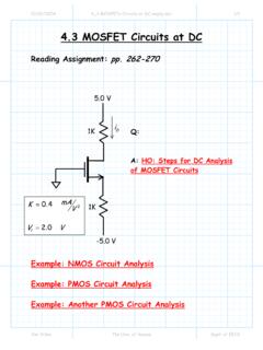
Transcription of Power MOSFET Basics: Understanding Gate Charge and …
1 VISHAY SILICONIXP ower MOSFETsDevice Application Note AN608 APower MOSFET basics : Understanding gate Chargeand Using it to Assess Switching NOTE Revision: 16-Feb-161 Document Number: 73217 For technical questions, contact: DOCUMENT IS SUBJECT TO CHANGE WITHOUT NOTICE. THE PRODUCTS DESCRIBED HEREIN AND THIS DOCUMENTARE SUBJECT TO SPECIFIC DISCLAIMERS, SET FORTH AT note is part of a series of application notes that definethe fundamental behavior of mosfets , both as standalonedevices and as switching devices implemented in a SwitchMode Power Supply (SMPS). Vishay Application NoteAN-605 [1] provides a basic description of the MOSFET andthe terminology behind the device, including definitions andphysical structure.
2 AN-850 [2] provides a broad, physicaldescription of the switching process. This application notegoes into more detail on the switching behavior of theMOSFET when used in a practical application circuit andattempts to enable the reader / designer to choose the rightdevice for the application using the minimum availableinformation from the datasheet. The note goes throughseveral methods of assessing the switching performance ofthe MOSFET and compares these methods againstpractical results. Several definitions used within the text aredrawn from application note THE MOSFET IN ISOLATIONU sing CapacitanceTo get a fundamental Understanding of the switchingbehavior of a MOSFET , it is best first to consider the devicein isolation and without any external influences.
3 Under theseconditions, an equivalent circuit of the MOSFET gate isillustrated in Fig. 1, where the gate consists of an internalgate resistance (Rg), and two input capacitors (Cgs and Cgd).With this simple equivalent circuit it is possible to obtain theoutput voltage response for a step gate voltage VGS is the actual voltage at the gate of thedevice, and it is this point that should be considered whenanalyzing the switching behavior. Throughout this noteupper case subscripts will refer to rated or applied voltagesand currents, while measured or time varying quantities willbe designated by lower case subscripts.
4 For example thevariable gate drain capacitance is designated as Cgd whileits corresponding Charge will be designated as QGD. If a step input is applied at VGS, then the following holds true:Fig. 1 - An Equivalent MOSFET gate CircuitShowing Just Cgs, Cgd, and Rg(1)(2)(3)Since VDS is fixed(4)therefore(5)and(6)VDSCgdCgsIgdIg sRgIgVGSVgsIgVGS- VgsRg------------------------=IgIgs + Igd=IgsCgs x dVgsdt-------------=IgdCgd x dVgsVDS dt----------------------------------== Cgd x dVgsdt-------------IgVGS- VgsRg------------------------Igs + Igd==IgCgsdVgsdt------------- + CgddVgsdt-------------=Cgs + Cgd =dVgsdt-------------dVgsVGS - Vgs--------------------------dtRg x Cgs + Cgd ---------------------------------------- -------= Power MOSFET basics .
5 Understanding gate Chargeand Using it to Assess Switching PerformanceDevice Application Note SiliconixAPPLICATION NOTE Revision: 16-Feb-162 Document Number: 73217 For technical questions, contact: DOCUMENT IS SUBJECT TO CHANGE WITHOUT NOTICE. THE PRODUCTS DESCRIBED HEREIN AND THIS DOCUMENTARE SUBJECT TO SPECIFIC DISCLAIMERS, SET FORTH AT (7)(8)at t = 0 s, VGS = 0 V, solving for K,(9)We define two parameters RG and Ciss to simplify theequations. RG is the effective total gate resistance definedas the sum of internal gate resistance Rg of the MOSFET andany external resistance Rgext that is part of the gate drivecircuitry.
6 Ciss is the effective input capacitance of theMOSFET as seen by the gate drive = Rg + Rgext and Ciss = Cgs + CgdRewriting equation (9) with effective values of gateresistance and capacitance In most cases the parameter of importance is not the actualgate voltage but the time taken to reach it.(10)While the RC circuit of Fig. 1 is rather simple, when theMOSFET is considered with additional parasitics, itbecomes increasingly difficult to manipulate theseequations manually. Therefore a method of analyzing apractical circuit is required. If the second order or parasiticcomponents are ignored, then it is possible to come up withanalytical solutions for formulas for the turn-on and turn-offtime periods of the MOSFET .
7 These are given in equations(11) through to (16) and the resulting waveforms are shownin Fig. 2 and Fig. 3. These equations are based on thosedeveloped in [3], VTH is the MOSFET threshold voltage, andVgp is the gate plateau 2 - Turn-On Transient of the MOSFET (11)(12)and(13)This gives accurate t1 and t2 when using datasheet values,but the time period t3 is difficult to calculate since Cgdchanges with Vds. During t3, gate voltage Vgs is constant atVgp and all of the gate current goes to discharge Cgd fromVDS to almost zero. The drain source voltage across theMOSFET when conducting full load current is considerednegligible compared to VDS voltage across the MOSFET when it is the same principles for turn-off, the formulas for theswitching transients are given below.
8 (14)(15)(16)-In VGS - Vgs tRg x Cgs + Cgd ---------------------------------------- -------K+=VgsVGS - K x e-tRg x Cgs + Cgd ---------------------------------------- ------=VgsVGS1 - e-tRg x Cgs + Cgd ---------------------------------------- ------ =e-tRGCiss------------------1 - VgsVGS----------=tRGCiss x 11 - VgsVGS------------------------------ ln=t1 VgsVTHVdsVgpIdst3t2 Timet1 RGCiss x 11 - VTHVGS------------------------------ ln=t2 RGCiss x 11 - VgpVGS------------------------------ ln=t3 RGCgd x VDSVGS - Vgp--------------------------=t4 RGCiss x VGSVgp---------- ln=t5 RGCgd x VDSVgp----------=t6 RGCissVgpVTH---------- ln
9 = Power MOSFET basics : Understanding gate Chargeand Using it to Assess Switching PerformanceDevice Application Note SiliconixAPPLICATION NOTE Revision: 16-Feb-163 Document Number: 73217 For technical questions, contact: DOCUMENT IS SUBJECT TO CHANGE WITHOUT NOTICE. THE PRODUCTS DESCRIBED HEREIN AND THIS DOCUMENTARE SUBJECT TO SPECIFIC DISCLAIMERS, SET FORTH AT this instance, t4 and t6 can be calculated accurately, but itis the formula for t5 which is more difficult to solve, sinceduring this time period VDS will change, causing Cgs to alsochange. Therefore some method is required to calculate t3and t5 without using the dynamic 3 - Turn-Off Transient of the MOSFETU sing gate Charge to Determine Switching TimeLooking at the gate Charge waveform in Fig.
10 4, QGS isdefined as the Charge from the origin to the start of the MillerPlateau Vgp; QGD is defined as the Charge from Vgp to theend of the plateau; and QG is defined as the Charge from theorigin to the point on the curve at which the driving voltageVGS equals the actual gate voltage of the device. [4]The rise in Vgs during t2 (Fig. 2) is brought about by chargingCgs and Cgd. During this time Vds does not change and assuch Cgd and Cds stay relatively constant, since they vary asa function of Vds. At this time Cgs is generally larger than Cgdand therefore the majority of drive current flows into Cgsrather than into Cgd.