Transcription of Precision 8-Channel / Dual 4-Channel CMOS Analog …
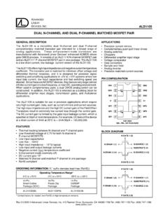
1 DG508B, Siliconix S14-2382-Rev. E, 15-Dec-141 Document Number: 64821 For technical questions, contact: DOCUMENT IS SUBJECT TO CHANGE WITHOUT NOTICE. THE PRODUCTS DESCRIBED HEREIN AND THIS DOCUMENTARE SUBJECT TO SPECIFIC DISCLAIMERS, SET FORTH AT 8-Channel / dual 4-Channel CMOS Analog MultiplexersDESCRIPTIONThe DG508B is an 8-Channel single-ended analogmultiplexer designed to connect one of eight inputs to acommon output as determined by a 3-bit binary address(A0, A1, A2). The DG509B is a dual 4-Channel differentialanalog multiplexer designed to connect one of fourdifferential inputs to a common dual output as determinedby its 2-bit binary address (A0, A1). Break-before-makeswitching action protects against momentary crosstalkbetween adjacent on channel conducts current equally well in bothdirections.
2 In the off state each channel blocks voltages upto the power supply rails. An enable (EN) function allows theuser to reset the multiplexer / demultiplexer to all switchesoff for stacking several devices. All control inputs,addresses (AX) and enable (EN) are TTL compatible over thefull specified operating temperature DG508B and DG509B are fabricated on an enhancedSG-II CMOS process that achieves improved performanceon: reduced charge injection, lower device leakage, andminimized parasitic capacitance. As the DG508, DG509 has a long history in the industry withmany suppliers offering copies - and in some casesimproved variations - with the best in class improvements,the vishay Siliconix new version of the DG508B, DG509 Bare the superior alternatives to what is currently for the DG508B, DG509B include high speedand high Precision data acquisition, audio signal switchingand routing, ATE systems, and avionics.
3 High performanceand low power dissipation make them ideal for batteryoperated and remote instrumentation DG508B and DG509B have the absolute maximumvoltage rating extended to 44 V. Additionally, single supplyoperation is also allowed. An epitaxial layer DG508B and DG509B are both available in 16-leadSOIC, TSSOP, PDIP, and miniQFN ( mm x mm)package options with extended temperature range of -40 Cto +125 more information, refer to vishay Siliconix DG508B,DG509B evaluation board Operate with single or dual power supply V+ to V- Analog signal swing range 44 V power supply maximum rating Extended operate temperature range:-40 C to +125 C Low leakage typically < 3 pA Low charge injection - QINJ = 2 pC Low power - ISUPPLY: 10 A TTL compatible logic > 250 mA latch-up current per JESD78 Available in SOIC16, TSSOP16, PDIP, and miniQFN16packages Superior alternative to: - ADG508A, DG508A, HI-508- ADG509A, DG509A, HI-509 Material categorization.
4 For definitions of complianceplease see BENEFITS Reduced switching errors Reduced glitching Improved data throughput Reduced power consumption Increased ruggedness Wide supply ranges ( 5 V to 20 V)APPLICATIONS Data acquisition systems Audio and video signal routing ATE systems Medical instrumentationDG508B, Siliconix S14-2382-Rev. E, 15-Dec-142 Document Number: 64821 For technical questions, contact: DOCUMENT IS SUBJECT TO CHANGE WITHOUT NOTICE. THE PRODUCTS DESCRIBED HEREIN AND THIS DOCUMENTARE SUBJECT TO SPECIFIC DISCLAIMERS, SET FORTH AT BLOCK DIAGRAM AND PIN CONFIGURATIONTRUTH TABLES AND ORDERING INFORMATIONL ogic 0 = VIL VLogic 1 = VIH 2 V X = Do not careS3A0S6DS4A1S8S7 ENDual-In-LineSOIC and TSSOPA2V-GNDS1V+S2S5 Decoders/Drivers123456716151413121110 Top viewTop view89DG508 BDual-In-LineSOIC and TSSOP9A0 DaA1 DbENGNDV-V+S1aS1bS2aS2bS3aS3bS4aS4bDecod ers/Drivers1234567161514131211108DG509 BminiQFN-16 LTop ViewDevice Marking: 6 XXTraceability Code:6 is DG508 BENXX = Date/LotDG508 BminiQFN-16 LDG509 BTop ViewDevice Marking: 7 XXTraceability Code:7 is DG509 BENXX = Date/LotPin 1: LONG LEAD13141516876512 3 412111096 XXDecoders/DriversV-S1S2S3S4S7S8DA2A1A0 ENS5S6V+GNDPin 1.
5 LONG LEAD13141516876512 3 412111097 XXDecoders/DriversV-S1AS2AS3AS4AS4 BDBGNDA1A0 ENS2BS3BV+DAS1 BTRUTH TABLE (DG508B)A2 A1 A0 EN ON SWITCH X X X 0 None 0 0 0 1 1 0 0 1 1 2 0 1 0 1 3 0 1 1 1 4 1 0 0 1 5 1 0 1 1 6 1 1
6 0 1 7 1 1 1 1 8 TRUTH TABLE (DG509B)A1 A0 EN ON SWITCH X X 0 None 0 0 1 1 0 1 1 2 1 0 1 3 1 1 1 4 DG508B, Siliconix S14-2382-Rev.
7 E, 15-Dec-143 Document Number: 64821 For technical questions, contact: DOCUMENT IS SUBJECT TO CHANGE WITHOUT NOTICE. THE PRODUCTS DESCRIBED HEREIN AND THIS DOCUMENTARE SUBJECT TO SPECIFIC DISCLAIMERS, SET FORTH AT -40 C to +85 C datasheet limits Signals on SX, DX or INX exceeding V+ or V- will be clamped by internal diodes. Limit forward diode current to maximum current All leads soldered or welded to PC Derate 8 mW/ C above 70 Derate mW/ C above 70 Derate mW/ C above 70 Derate mW/ C above 70 INFORMATION (DG508B)TEMP. RANGEPACKAGEPART NUMBER-40 C to +125 C a16-Pin SOICDG508 BEY-T1-E316-Pin TSSOPDG508 BEQ-T1-E316-Pin PDIPDG508 BEJ-E316-Pin MiniQFNDG508 BEN-T1-GE4 ORDERING INFORMATION (DG509B)TEMP. RANGEPACKAGEPART NUMBER-40 C to +125 C a16-Pin SOICDG509 BEY-T1-E316-Pin TSSOPDG509 BEQ-T1-E316-Pin PDIPDG509 BEJ-E316-Pin MiniQFNDG509 BEN-T1-GE4 ABSOLUTE MAXIMUM RATINGSPARAMETER LIMITUNIT Voltages Referenced to V- V+44 VGND25 Digital Inputs a, VS, VD(V-) - 2 to (V+) + 2or 20 mA, whichever occurs firstCurrent (Any terminal) 30mAPeak Current, S or D (Pulsed at 1 ms, 10 % duty cycle max.)
8 100 Storage Temperature (EY, EQ, EJ, EN suffix)-65 to +150 CPower Dissipation (Packages) b16-Pin Narrow SOIC c600mW16-Pin TSSOP d45016-Pin PDIP e51016-Pin miniQFN f525 Thermal Resistance ( JA) b 16-Pin Narrow SOIC c125 C/W16-Pin TSSOP d17816-Pin PDIP miniQFN f152DG508B, Siliconix S14-2382-Rev. E, 15-Dec-144 Document Number: 64821 For technical questions, contact: DOCUMENT IS SUBJECT TO CHANGE WITHOUT NOTICE. THE PRODUCTS DESCRIBED HEREIN AND THIS DOCUMENTARE SUBJECT TO SPECIFIC DISCLAIMERS, SET FORTH AT SYMBOL TEST CONDITIONS UNLESS OTHERWISE SPECIFIED V+ = 15 V, V- = -15 V ( 10 %)VAX, VEN = 2 V, V aTEMP. b TYP. c-40 C to +125 C -40 C to +85 CUNIT MIN. d MAX. dMIN. d MAX. dAnalog SwitchAnalog Signal Range eVANALOGFull--1515-1515 VDrain-Source On-ResistanceRDS(on)VD = 10 V, IS = -1 mARoom180-380-380 Full--480-450 RDS(on) Matching RDS(on)VD = 10 VRoom10----Source Off Leakage CurrentIS(off)VD = 10 V VS = 10 VVEN = 0 V Room--11-11nAFull--5050-5050 Drain Off Leakage CurrentID(off)DG508 BRoom--11-11 Full--100100-100100DG509 BRoom--11-11 Full--5050-5050 Drain On Leakage CurrentID(on)
9 VS = VD = 10 V sequence each switch on DG508 BRoom--11-11 Full--100100-100100DG509 BRoom--11-11 Full--5050-5050 Digital ControlLogic High Input VoltageVINHFull-2-2-VLogic Low Input High Input CurrentIIHVAX, VEN = 2 VFull--11-11 ALogic Low Input CurrentIILVAX, VEN = VFull--11-11 Logic Input Capacitance eCINf = 1 MHzRoom4----pFDynamic CharacteristicsTransition TimetTRANSVS1 = +10 V/-10 V, VS8 = -10 V/+10 V, RL = 1 M , CL = 35 pFRoom145-300-300nsFull--400-400 Break-Before-Make IntervaltOPENVS1 = VS8 = 5 V, CL = 35 pF, RL = 1 k Room3715-15-Full-1-1-Enable Turn-On TimetON(EN)VS1 = 5 V, VS2 to VS8 = 0 V, RL = 1 k , CL = 35 pFRoom100-250-250 Full--340-340 Enable Turn-Off TimetOFF(EN)Room90-240-240 Full--300-300 Charge Injection eQINJCL = 1 nF, RGEN = 0 W, VGEN = 0 VFull2----pCOff Isolation eOIRRCL = 5 pF, RL = 50 , f = 1 MHzRoom-81----dBCrosstalk eXTALKRoom-88-----3 dB Bandwidth eBWRL = 50 Room250----MHzTotal HarmonicDistortion eTHDRL = 10 k , 5 Vrmsf = 20 Hz to 20 Off Capacitance eCS(off)f = 1 MHzRoom3----pFDrain Off Capacitance eCD(off)DG508 BRoom13----DG509 BRoom8----Drain On Capacitance eCD(on)DG508 BRoom18----DG509 BRoom11----Power SupplyPositive Supply CurrentI+VAX, VEN = V or Supply A + + DG508B, Siliconix S14-2382-Rev.
10 E, 15-Dec-145 Document Number: 64821 For technical questions, contact: DOCUMENT IS SUBJECT TO CHANGE WITHOUT NOTICE. THE PRODUCTS DESCRIBED HEREIN AND THIS DOCUMENTARE SUBJECT TO SPECIFIC DISCLAIMERS, SET FORTH AT (Single Supply 12 V)PARAMETER SYMBOL TEST CONDITIONS UNLESS OTHERWISE SPECIFIED V+ = 12 V, V- = 0 V ( 10 %)VAX, VEN = 2 V, V aTEMP. bTYP. c-40 C to +125 C -40 C to +85 CUNIT MIN. d MAX. dMIN. d MAX. dAnalog SwitchAnalog Signal Range eVANALOGFull-012012 VOn-ResistanceRDS(on)VD = 10 V/0 V, IS = 1 mARoom265-500-500 Full--650-600 RDS(on) Matching RDS(on)Room10----Switch Off Leakage CurrentIS(off)V+ = 12 V, V- = 0 VVD = 0 V/10 V, VS = 10 V/0 VRoom--11-11nAFull--50-50-5050ID(off)DG5 08 BRoom--11-11 Full--100100-100100ID(off)DG509 BRoom--11-11 Full--5050-5050 channel On Leakage CurrentID(on)