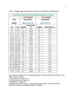
Transcription of Section 5 High Speed PCB Layout Techniques
1 High Speed Analog Design and Application Seminar5-1 texas InstrumentsSection 5 High Speed PCB Layout TechniquesScenario: You have spent several days, no maybe weeks, perfecting adesign on paper and also using Spice to ensure the design exceeds allexpectations. You hand the schematic to your Layout person who puts alleverything on a printed circuit board (PCB). The PCB comes back in a weekor two and is finally populated and ready to test. But it doesn t work!!!!Why not? On paper it works!! Spice said it works!! But it doesn t work!!This scenario happens more often than not and the reason many circuits donot work as expected is due primarily to the PCB Section looks at some key fundamentals of high Speed PCB layouttechniques so that hopefully the above scenario will never happen to Speed Analog Design and Application Seminar5-2 texas InstrumentsPCB Components + twhlnL(nH) () ++ twhlnrC(pF) htw rComponent: Copper TracesPurpose: Interconnect two or more pointsProblem: Inductance and Capacitancex = length of trace (cm)w = width of trace (cm)h = height of trace (cm)t = thickness of trace (cm)er = PCB ( ) trace on ( ) thick PCB (FR-4) has.
2 4nH and per cm 10nH and per inchL(nH)C(pF))ps/cm( ()C(pF)L(nH) er = PCB materialpermeability (FR-4 )The PCB consists of layers of metal and insulator and can consist ofseveral layers. Examining some common elements of a PCB will help thereader understand what many people believe is Black Magic .Copper traces are utilized to connect one element node to another shape of these traces determine one very important aspect of a PCB the characteristic inductance, capacitance, and ultimately thecharacteristic impedance. Resistance is generally ignored as most designsdo not carry more than several mA of current and the results can often impedance (Z0) was covered previously, so this will not bediscussed here. But what is important is the inductance and capacitanceas determined by the trace dimensions and the PCB dielectric ( r).
3 FR-4,probably the most common PCB material used by manufacturers todayand has a permeability range normally from to , but is oftenused as a typical permeability. Check with the PCB manufacturer todetermine what material they utilize and the associated : Reference the book entitled High- Speed Digital Design AHandbook for Black Magic written by Howard Johnson and MartinGraham, 1993, Prentice-Hall, ISBN Speed Analog Design and Application Seminar5-3 texas instruments (pF)A r Component: Copper PlanesPurpose: Used For Ground Planes and Power PlanesProblem: Stray Capacitance on Signal TracesBenefit: Large Bypass Capacitance & Minimal Inductanceh = separation between planes (cm)A = area of common planes = l*w (cm2)er = PCB ( ) thick PCB (FR-4) has.
4 Per cm2 per inch2h rwlAer = PCB materialpermeability (FR-4 )PCB ComponentsCopper planes are typically found when power planes and ground planesare utilized. Planes make an excellent high frequency capacitor and canoften be utilized for high frequency bypassing in complement withtraditional use of a solid ground plane is generally preferred over a grid plane. Asolid plane minimizes inductance to the absolute minimum which is adesirable trait for high Speed signals which includes both Analog andDigital signals. But, as will be discussed later, this plane can causecapacitance problems to sensitive nodes of the circuit. Be aware of allattributes of the circuit and do not blindly use planes side benefit of a solid plane is it becomes a very good thermal conductorand can act as a heat sink to keep thermal levels of all devices on the flip side, temperature sensitive components may not want tohave the ground plane nearby due to this heat Speed Analog Design and Application Seminar5-4 texas ( ) via with ( ) thick PCB has ( ) Clearance hole around ( ) pad on FR-4 has : ViasPurpose: Interconnect traces on different layersProblem: Inductance and CapacitancePCB Components + dhlnhL(nH)415121 05550ddd h C(pF)r.
5 Er = PCB material permeability (FR-4 )L(nH)C(pF))ps/cm( ()C(pF)L(nH) Vias are utilized to simplify trace routing around other components or whenthere is a high density of interconnections to be made ( BGApackages). Just as a PCB trace had inductance and capacitance, so todoes a via. Generally these elements are ignored as the length of the viasare typically very small relative to the rest of the trace. But, this Can causeissues if the signals are very high frequency (>100 MHz) or have energy /harmonics at high easiest way to minimize problems of a via is to simply not use themwith signal traces. At the very least it should be minimized. If vias must beused, there are other issues to worry about that will be discussed Speed Analog Design and Application Seminar5-5 texas Instrumentshtw rD 21 + =hD1h Ii(A/cm)O i(A/cm)IO = total signal current (A)h = height of trace (cm)D = distance from trace (cm)Current Density Illustrates Return Current Flow is directly below thesignal trace.
6 The creates the path of least impedance. Must have Solid return path ( Solid Ground Plane)under the signal trace to maintain homogeneous natureof current density is the concentration of current flowing through a is especially important when looking at return thing that many people forget about is for a current to flow out to apoint, there MUST be a return path or else current will Not flow. Sincethere is a current flow, then the return current flow will find a way back toits source one way or another. Return current density is highest directlyunder (or over) the signal trace it was sourced from. Even if a solid groundplane is used, the concentration of current flow will still be adjacent to thesignal source Speed Analog Design and Application Seminar5-6 texas InstrumentsHigh Frequency Input Current PathRTERMVia to BottomGND PlaneViaTop LayerCurrent FlowBotttom LayerCurrent FlowRTERMVia to BottomGND PlaneViaRTERMVia to BottomGND PlaneViaBreak in GNDP lanePicks upHF ReturnThruReference+-NOISEBADL argeCurrent LoopBETTERR educedCurrent LoopBESTM inimum CurrentLoopHigh Frequency Current Paths Always Follow thePath of Least Impedance - Not Current Loop +Discontinuous GNDP laneRTERM+-NoNoiseReferenceis Quiet As just discussed, the lowest impedance path of a high Speed signal is directlyunder a PCB trace.
7 This minimizes the current loop area substantially. The worst case scenario shows a long winding trace creates a large current loop area which ismade even worse by the break in the ground plane. The obvious issue with this isthe ground plane is often used as a reference point for other parts of the system. Ifthe current flow density is high near one of these reference points, this can (andoften does) cause noise to occur in the circuit and often propagates throughout theentire signal the bad Layout shows, also shows a long winding trace that does not follow the shortest distance between two points is a straight line method. The better layoutminimizes the distance while reducing the current loop area. But, the best way to dothe Layout is to place the receiver part as close as possible to the input.
8 This easilyis the smallest loop area and delays in the signal path are drastically reduced. A keybenefit of this method is the reference ground point for other circuits are kept quiet and should have no contribution from the undesirable current also minimizes the need for adhering to strict strip-line Techniques as the signalpath acts as a lumped circuit and not a distributed circuit. A lumped circuit typicallyhas rising edges much less than the delay time of the transmission line, thusminimizing issues. The construction of transmission lines naturally keeps the sourceand return currents close to each other. This helps minimize current loop area anddrastically reduces noise along the path on the PCB and also Speed Analog Design and Application Seminar5-7 texas InstrumentsRSOURCE+VS-VSHigh Frequency Output Current PathProblems: Long winding path causinglarge current loop area.
9 HF bypass caps are placedtoo far away from amplifierand GND. Inductanceeliminates benefit of bypasscaps. GND of bypass caps are toofar away from amplifieroutput. Series Resistor (RSOURCE)is too far away from theamplifier. Causes C-loadingon amplifier and lack of atransmission line. Single GND point onconnectorLooking at the Output current path shows the exact same phenomenon as theinput current flow the return current path will follow the signal trace pathwherever it may go. One issue that is often overlooked is where does thisreturn current flow once it reaches the output of the driver? As we all know,current must close the loop or else there is no current the example above, the return current flows through the bypass capacitorsand back into the power supply lines.
10 Now we see that the bypass capacitorsare part of the loop and will have impact on the performance of the it makes sense to place the capacitors as close as possible to thedriver power supply pins and the actual output issue with the above system is the source resistance is very far awayfrom the driver. As will be discussed later, this is a bad thing for the driver andmay cause stability problems. Additionally, the transmission line typicallystarts at the load side of the resistor. This system may have a undefinedcharacteristic impedance that may cause reflection last concern is the single ground connection point of the connector. Thismay cause a significant impedance mismatch in the return current Speed Analog Design and Application Seminar5-8 texas InstrumentsHigh Frequency Output Current PathSolutions: Amplifier is next to Connectorminimizing loop area.