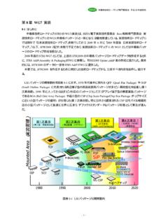
Transcription of 低密度実装を可能にする ... - semicon.jeita.or.jp
1 1 Work in Progress - Do not publishSTRJ WS: March 2, 2012, WG7 ( ) 2011 STRJ 2011 3 2 ( ) STRJ WG7 ( ) 2 Work in Progress - Do not publishSTRJ WS: March 2, 2012, WG7 ( ) 2011 6 2011 7 2012 2 ASET 2011 10 2011 STRJ WG7 3 Work in Progress - Do not publishSTRJ WS: March 2, 2012, WG7 ( )Application(Products)PWBP assiveComponentsDesignTESTI nter-connectLitho PIDS FEP ES&HM&SMET ERD ERM FI AssemblyEquipmentsPackageMEMSS emiconductor Technology Roadmap committee (STRJ)Semiconductor Technology Roadmap committee (STRJ)Japan Jisso Technology Roadmap committee (JJTR)Japan Jisso Technology Roadmap committee (JJTR)JEITAJEITA JJTR WG3 STRJ WG7 SeedsNeedsSTRJ WG7 4 Work in Progress - Do not publishSTRJ WS: March 2, 2012, WG7 ( ) mobilityHarshenvironmentHighHighAutomoti ve electronicsCar navigation CellphoneNote PC Mobile digital imaging Wearable Home digital AV 2011 5 Work in Progress - Do not publishSTRJ WS.
2 March 2, 2012, WG7 ( ) 11 WGWG (STRJ) (JJTR)2011 ITRS 2011 2012 1 ITRS 2010 STRJ ITRS ITRS A&P TWG ECTC ITRS A&P TWG ITRS A&P TWG ITRS Jan. 2011 IITRS 2011 2011 5 2011 WG JJTR ASET TSV WG5 LED IMSI WLP Mar. 2011 Apr. 2011 May, 2011 July, 2011 Aug. 2011 Oct. 2011 Dec. 2011 Feb. 2011 Feb. 2012 2013 ITRS2011 6 Work in Progress - Do not publishSTRJ WS: March 2, 2012, WG7 ( )1) ITRS 2011 2011 8 1 SiP 2) ( ) 8 3 ITRS Package Workshop ITRS 3 STRJ 4 jeita 4 20 31 3) WG 3 LSI ( ) IMSI ( LED ( ) 3D-TSV ASET ( : ASET) 11 WGWG ITRS 2011 Package 7 Work in Progress - Do not publishSTRJ WS: March 2, 2012, WG7 ( ) 2007 2011 8 Work in Progress - Do not publishSTRJ WS.
3 March 2, 2012, WG7 ( ) Tr Cu (1)(2) Ultra Low k Low k (Chip-package interaction) (3) TSV TSV (4) (5) T/C (6) Ta=175 C (6)9 Work in Progress - Do not publishSTRJ WS: March 2, 2012, WG7 ( )(1) (1) / 10 Work in Progress - Do not publishSTRJ WS: March 2, 2012, WG7 ( ) Tables treat SiTables treat Si--Intermediate, SiIntermediate, Si--base and glass base and glass Interposers separatelyInterposers separatelyTSV Key Technical Parameters for InterposersIntermediate Silicon InterposerYear of Production201120122013 Minimum TSV pitch (um) TSV diameter (um) (D) maximum aspect ratio (L/D)101010 Minimum Si Wafer final thickness (um)403020 TSV Methods and Materialssee table AP14 Via fill methodCu ECD FillCu ECD Fill Cu ECD FillTSVTSV metalCuCuCuConstruction compatibilitysee interposer cross-sections Alignment requirement (um) (assume 25% exit dia) of RDL Layers Front side222 Number of RDL Layers Back side2223D IntegrationInterconnect methodsCu-Cu, Cu-Sn-Cu, Cu-Ni/Au-SnAg, AuSnCu-Cu, Cu-Sn-Cu, Cu-Ni/Au-SnAg, AuSnCu-Cu, Cu-Sn-Cu, Cu-Ni/Au-SnAg, AuSn11 Work in Progress - Do not publishSTRJ WS.
4 March 2, 2012, WG7 ( )(2) (2) CuCu Sn95Pb bumpSnAgCu/SnAg bumpCu pillar + SnAg cap 130um ( 12 Work in Progress - Do not publishSTRJ WS: March 2, 2012, WG7 ( ) CuCu 0501001502002502009 2010 2011 2012 2013 2014 2015 2016 2017 2018 2019 2020 Bump pitch (um)Low costHandheldHighperformance Peripheral Solder bumpCu pillar 2011 13 Work in Progress - Do not publishSTRJ WS: March 2, 2012, WG7 ( ) Capillary underfill NCP/ACP NCF/ACF No flow Underfill Mold underfill Wafer-level underfill Pre-applying methodUnderfillSolder bumpSolderSubstrateUnderfillAu bumpSolderSubstratemetal fillerUnderfillSubstrateBumpUnderfillSub strateBumpSolder bumpNCF/NCPAu-solderACF/ACPS ubstrateSolder UnderfillCu-solderCu pillar Wafer- level underfill 14 Work in Progress - Do not publishSTRJ WS: March 2, 2012, WG7 ( )(3) (3) Low k Low k (CPI)(CPI)Cu low k 15 Work in Progress - Do not publishSTRJ WS.)
5 March 2, 2012, WG7 ( )Low k Low k (white bump)(white bump) FEMFEM Energy release rate (ERR) 16 Work in Progress - Do not publishSTRJ WS: March 2, 2012, WG7 ( )(4)(4) TSVTSV Cu-TSV XY TSV 2 Keep out zone TSV TSV Z Cu-Cu TSV drtg r t Cu-TSV Tr Tr TSV SiliconCu-TSV17 Work in Progress - Do not publishSTRJ WS: March 2, 2012, WG7 ( )(5)(5) Source: Dan Tracy, Semi, Semicon Taiwan Cost RatioAu wirePd-CuwirePure Cuwire 7 3 18 Work in Progress - Do not publishSTRJ WS: March 2, 2012, WG7 ( )StaggeredIn-line 2016 (5)(5) 010203040506070201020122014201620182020A u wire, singleCu wire, singleAu wire, staggeredCu wire, staggeredAl splashSource: JJTR 2011 19 Work in Progress - Do not publishSTRJ WS: March 2, 2012, WG7 ( )(6)(6) 1.
6 Power Train1. Power TrainEngine/motorAT controlBattery 5. SafetyPredictive mechanismABS, air bagStability controlMonitoring a driverChassisSuspensionElectric power steering2. NetworkingCANFlexRayMOST3. Information &Mobile CommunicationGPS NavigationEntertainmentService4. Body & SecurityAir conditioningCipher door lockPower windowIntelligent beamAudio 20 Work in Progress - Do not publishSTRJ WS: March 2, 2012, WG7 ( ) Unit201020122014201620182020 C125125125125125125 -Si-MOSFETSi-IGBTSi-MOSFET, Si-IGBTSiC-MOSFET, GaN-MOSFET C 175200210240280300 W/cm32610162330 Package resistancem C175200200200200200 (W/cm3) at 125 C. C155155155155175175 C175175175175200200 -Al pad OPMOPMOPM OPM OPM -Au wireAu wireAu/CuAu/CuAu/CuAu/Cu 21 Work in Progress - Do not publishSTRJ WS: March 2, 2012, WG7 ( )~ ~ ~ wireAu wireDieLead Frame(Source,Gate)Au WireDie pad(Drain) Lowering Ron Reduction of Interconnection resistance Reduction of Interconnection resistance Al ribbonCu clipThick Cu wireCu-Si-Cu stack22 Work in Progress - Do not publishSTRJ WS: March 2, 2012, WG7 ( ) 0100200300400500600700201020122014201620 182020 x 10 (W/cm3) (A/cm2) (deg C) ( C) x 10 (deg C/W)Introduction of SiC/GaNSiC ( ) 23 Work in Progress - Do not publishSTRJ WS.
7 March 2, 2012, WG7 ( ) TSV TSV