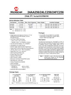
Transcription of Si4010-C2 Data Sheet - Silicon Labs
1 S i4010- C2. C R Y S T A L- L E S S S O C R F T R A N S M I T T E R. Features Crystal-less operation Single Coin-Cell Battery Operation Optional crystal oscillator input Supply voltage: to V. High-Speed 8051 C Core Standby current < 10 nA. Pipeline instruction architecture High-performance RF transmitter 70% of instructions in 1 or 2 clocks Frequency range: 27 960 MHz Up to 24 MIPs with 24 MHz clock +10 dBm output power, 4 kB RAM/8kB NVM adjustable 128 bit EEPROM Automatic antenna tuning 256 byte of internal data RAM Symbol rate up to 100 kbps 12 kB ROM embedded functions FSK/OOK modulation 8 byte low leakage RAM Manchester, NRZ, 4/5 encoder Extensive Digital Peripherals Analog Peripherals 128 bit AES accelerator LDO regulator with POR circuit 5/9 GPIO with wakeup functionality Battery voltage monitor LED driver Temperature range 40 to +85 C.
2 Data serializer Automotive quality option, High-speed frequency counter AEC-Q100. On-chip debugging: C2. 10-pin MSOP/14-pin SOIC. Unique 4 byte serial number Ultra low-power sleep timer Ordering Information: See page 15. Applications Garage and gate door openers Home automation and security Pin Assignments Remote keyless entry Wireless remote controls Description The Si4010 is a fully integrated crystal-less CMOS SoC RF transmitter with an embedded CIP-51 8051 MCU. The device can operate over the 40 to 85 C. temperature range without requiring an external crystal reference source reducing board area and BOM cost. The device includes an 8 kB non volatile memory block for programming the user's application along with a 12 kB ROM of embedded support code for use in the user's application.
3 The Si4010 includes Silicon 10-Pin MSOP. Laboratories' 2-wire C2 Debug and Programming interface, which allows customers to download their code during the development stage into the on-board RAM for testing and debug prior to programming the NVM. The Si4010 is designed for low power battery applications with standby currents of less than 10 nA to optimize battery life and features automatic wake on button press support to efficiently move from the standby to active mode state with minimal customer code support. Built in AES-128 hardware encryption along with a 128-bit EEPROM can be used to create robust data encryption of the transmitted packets. A unique 4-byte serial number is programmed into each device ensuring non-overlapping device identifiers. The RF transmitter features a high efficiency PA capable of delivering output 14-Pin SOIC.
4 Power up to +10 dBm and includes an automatic antenna tuning algorithm. This algorithm adjusts the antenna tuning at the start of each packet transmission for optimal output power minimizing the impact of antenna impedance changes due Patents pending to the remote being held in a user hand. The devices supports FSK and OOK. modulations and includes automatic output power shaping to reduce spectral spreading and ease regulatory compliance. The output frequency can be adjusted via software over the entire 27 to 960 MHz range. The output data rate is software adjustable up to a maximum rate of 100 kbps. Rev. 8/20 Copyright 2020 by Silicon Laboratories Si4010. Si4 010- C2. Functional Block Diagram 2 Rev. S i4 0 1 0 -C 2. TA B L E O F C O N T E N T S. 1. System Overview.
5 11. 2. Test Circuit..13. 3. Typical Application Schematic ..14. Si4010 Used in a 5-Button RKE System with LED Indicator ..14. Si4010 with an External Crystal in a 4-Button RKE System with LED Indicator ..14. 4. Ordering Information ..15. 5. Top Markings ..16. SOIC ..16. MSOP..17. 6. Pin Definitions ..18. MSOP, Application ..18. MSOP, Programming/Debug Mode ..19. SOIC Package, Application ..20. SOIC Package, Programming/debug Mode..21. 7. Package Specifications ..22. 10-Pin MSOP ..22. 14-pin SOIC Package ..23. 8. PCB Land Pattern 10-Pin MSOP ..24. 9. PCB Land Pattern 14-pin SOIC Package..26. 10. Electrical Characteristics ..28. 11. System Description..33. Overview ..33. Setting Basic Si4010 Transmit Parameters ..35. Applications Programming Interface (API) Commands.
6 35. 12. Power Amplifier ..36. Register Description..38. 13. Output Data Serializer (ODS) ..40. Description ..40. Timing ..40. Register Description..41. 14. LC Oscillator (LCOSC) ..46. Register Description..46. 15. Low Power Oscillator and System Clock Generator ..47. Register Description..47. 16. Crystal Oscillator (XO) ..49. Register Description..50. 17. Frequency Counter ..51. Register Description..53. 18. Sleep Timer ..55. 19. Bandgap and LDO ..55. 20. Low Leakage HVRAM ..55. 21. Temperature Sensor ..55. 22. CIP-51 Microcontroller ..56. Rev. 3. Si4010-C2 . Instruction Set.. 57. Instruction and CPU Timing .. 57. CIP-51 Register Descriptions .. 62. 23. Memory Organization .. 66. Program Memory .. 67. Internal Data Memory .. 67. External Data Memory .. 67. General Purpose Registers.
7 67. Bit Addressable Locations .. 68. Stack.. 68. Special Function Registers (SFR) .. 68. Registers Mapped to XDATA Address Space (XREG).. 68. NVM (OTP) Memory .. 68. MTP (EEPROM) Memory .. 69. 24. System Boot and NVM Programming .. 70. Startup Overview .. 70. Reset .. 71. Chip Program Levels .. 71. NVM Organization .. 72. Device Boot Process .. 73. Error Handling During Boot.. 74. CODE/XDATA RAM Address Map .. 74. Boot Status Variables .. 77. Boot Routine Destination Address Space.. 80. NVM Programming .. 81. Retest and Retest Configuration.. 82. Boot and Retest Protection NVM Control Byte .. 84. Chip Protection Control Register .. 85. 25. On-Chip Registers .. 86. Special Function Registers .. 86. XREG Registers .. 89. 26. Interrupts .. 92. MCU Interrupt Sources and Vectors.
8 93. Interrupt Priorities .. 93. Interrupt Latency.. 93. Interrupt Register Descriptions .. 94. External Interrupts .. 100. 27. Power Management Modes.. 102. Idle Mode .. 102. Stop Mode .. 102. 28. AES Hardware Accelerator .. 104. AES SFR Registers .. 104. 29. Reset Sources .. 107. Device Boot Outline .. 107. External Reset .. 107. 4 Rev. Si4010-C2 . Software Reset .. 108. 30. Port Input/Output .. 109. GPIO Pin Special Roles .. 112. Pullup Roff Option.. 113. Matrix Mode Option .. 113. Pullup Roff and Matrix Mode Option Control .. 115. Special GPIO Modes Control .. 116. LED Driver on GPIO[5] .. 118. 31. Clock Output Generation .. 124. Register Description .. 125. 32. Control and System Setting Registers .. 127. 33. Real Time Clock Timer .. 129. RTC Interrupt Flag Time Uniformity.
9 130. Register Description .. 130. 34. Timers 2 and 3 .. 132. Interrupt Flag Generation .. 133. 16-bit Timer with Auto Reload (Wide Mode).. 134. 16-bit Capture Mode (Wide Mode) .. 134. 8-Bit Timer/Timer Mode (Split Mode) .. 135. 8-Bit Capture/Capture Mode (Split Mode) .. 136. 8-Bit Timer/Capture Mode (Split Mode) .. 137. 35. C2 Interface .. 149. C2 Pin Sharing .. 149. 36. IDE Development Environment and Debugging Chain .. 152. Functionality Limitations While Using IDE Development Environment .. 152. Chip Shutdown Limitation .. 153. LED Driver Usage while Using IDE Debugging Chain .. 153. 37. Additional Reference Resources .. 155. Document Change List .. 156. Contact Information.. 157. Rev. 5. Si4 010- C2. LIST OF FIGURES. Figure Si4010 Block Diagram .. 12. Figure Test Block Diagram with 10-Pin MSOP.
10 13. Figure Si4010 Used in a 5-button RKE System with LED Indicator .. 14. Figure Si4010 with an External Crystal in a 4-button RKE System with LED Indicator .. 14. Figure Si4010 Top Marking .. 16. Figure Si4010 Top Marking .. 17. Figure 10-Pin MSOP Package .. 22. Figure 14-Pin SOIC Package .. 23. Figure 10-Pin MSOP Recommended PCB Land Pattern .. 24. Figure 14-Pin SOIC Recommended PCB Land Pattern .. 26. Figure Functional Block Diagram .. 33. Figure Simplified PA block Diagram .. 36. Figure OOK Timing Example .. 40. Figure FSK Timing Example .. 40. Figure Frequency Counter Block Diagram .. 51. Figure CIP-51 Block Diagram .. 56. Figure Address Space Map after the Boot .. 66. Figure NVM Address Map .. 73. Figure CODE/XDATA RAM Address Map .. 76. Figure Boot Routine Destination CPU Address Space for Copy from NVM.