Transcription of SM3 - sinopowersemi.com
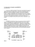
1 dual N- channel enhancement Mode reserves the right to make changes to improve reliability or manufacturability without notice, andadvise customers to obtain the latest version of relevant information to verify before placing Sinopower Semiconductor, - December, 2017 Pin DescriptionOrdering and Marking InformationFeaturesApplications Power Management in Desktop Computer or DC/DC MOSFETNote : SINOPOWER lead-free products contain molding compounds/die attach materials and 100% matte tin platetermination finish; which are fully compliant with RoHS. SINOPOWER lead-free products meet or exceed the lead-free requirements of IPC/JEDEC J-STD-020D for MSL classification at lead-free peak reflow temperature. SINOPOWER defines Green to mean lead-free (RoHS compliant) and halogen free (Br or Cl does not exceed 900ppm by weightin homogeneous material and total of Br and Cl does not exceed 1500ppm by weight).
2 S2G2(8)G1(1)D1(3)S1 / D2(4)(2)(5)(6)(7)(9) channel 130V/24A,RDS(ON) = (max.) @ VGS = 10 VRDS(ON) = (max.) @ VGS = channel 230V/44A,RDS(ON) = (max.) @ VGS =10 VRDS(ON) = 2mW (max.) @ VGS = 100% UIS + Rg Tested dual Dies Package and Minimize Board Space Lower Qg and Qgd for High-Speed Switching Lower RDS(ON) to Minimize Conduction Losses Reliable and Rugged Lead Free Available (RoHS Compliant)G1D1D1G2S1/D2S1/D2S1/D2S1/D2 DFN5x6G-8_EP2S2D1(Pin 9)SM7341 EHHandling CodeTemperature RangePackage CodePackage Code KP : DFN5x6G-8_EP2 Operating Junction Temperature Range C : -55 to 150 oCHandling Code TR : Tape & ReelAssembly Material G : Halogen and Lead Free DeviceSM7341EH KP :7341 EHXXXXXXXXXX - Lot CodeAssembly Sinopower Semiconductor, - December, 2017 Symbol Parameter channel 1 channel 2 Unit Common Ratings VDSS Drain-Source Voltage 30 V VGSS Gate-Source Voltage 20 V TJ Maximum Junction Temperature 150 C TSTG Storage Temperature Range -55 to 150 C IS Diode Continuous Forward Current TC=25 C 15 30 A ID Continuous Drain Current TC=25 C 73 186 A TC=100 C 46 118 IDM a Pulse Drain Current TC=25 C 100 200 A PD Maximum Power Dissipation TC=25 C 31 W TC=100 C 25 RqJC Thermal Resistance-Junction to Case Steady State 4 2 C/W ID b Continuous Drain Current TA=25 C 24 44 A TA=70 C 19 35 IDM Pulse Drain Current(T=300uS)
3 TA=25 C 60 110 A PD b Maximum Power Dissipation TA=25 C W TA=70 C RqJA b,c Thermal Resistance-Junction to Ambient t 10s 35 35 C/W Steady State 75 75 RqJA d Thermal Resistance-Junction to Ambient Steady State 120 120 C/W IAS e Avalanche Current, Single pulse L= 24 50 A EAS e Avalanche Energy, Single pulse L= 28 125 mJ Note a Pulse width is limited by max. junction temperature. Note b t 10s and surface mounted on FR-4 board using 1in2 pad, 2 oz Cu. Note c Steady time = 999s and surface mounted on FR-4 board using 1in2 pad, 2 oz Cu. Note d Steady time = 999s and surface mounted on FR-4 board and the minimum pad size of PCB. Note e UIS tested and pulse width are limited by maximum junction temperature 150oC(initial temperature Tj=25oC).
4 Absolute Maximum Ratings (TA = 25 C unless otherwise noted) Sinopower Semiconductor, - December, 2017 channel 1 Electrical Characteristics (TA = 25 C unless otherwise noted)Symbol Parameter Test Conditions channel 1 Unit Min. Typ. Max. Static Characteristics BVDSS Drain-Source Breakdown Voltage VGS=0V, IDS=250mA 30 - - V BVDSSt Drain-Source Breakdown Voltage (transient) VGS=0V, ID(aval)=24A Tcase=25 C, ttransient=100ns 34 - - V IDSS Zero Gate Voltage Drain Current VDS=24V, VGS=0V - - 1 mA TJ=85 C - - 30 VGS(th) Gate Threshold Voltage VDS=VGS, IDS=250mA V IGSS Gate Leakage Current VGS= 20V, VDS=0V - - 10 mA RDS(ON) f Drain-Source On-state Resistance VGS=10V, IDS=15A - mW TJ=125 C - - VGS= , IDS=12A - 5 Gfs Forward Transconductance VDS=5V, IDS=6A - 17 - S Diode Characteristics VSD f Diode Forward Voltage ISD=15A, VGS=0V - V trr Reverse Recovery Time ISD=15A, dlSD/dt=100A/ms Vdd=15V - 28 - ns ta Charge Time - 14 - tb Discharge Time - 14 - Qrr Reverse Recovery Charge - 13 - nC Dynamic Characteristics g RG Gate Resistance VGS=0V,VDS=0V,F=1 MHz - - W Ciss Input Capacitance VGS=0V, VDS=15V, Frequency= - 925 - pF Coss Output Capacitance - 550 - Crss Reverse Transfer Capacitance - 46 - td(ON) Turn-on Delay Time VDD=15V, RL=15W, IDS=1A, VGEN=10V, RG=1W - 11 - ns tr Turn-on Rise Time - - td(OFF)
5 Turn-off Delay Time - 21 - tf Turn-off Fall Time - 19 - Gate Charge Characteristics g Qg Total Gate Charge VDS=15V, VGS=10V, IDS=20A - 15 20 nC Qg Total Gate Charge VDS=15V, VGS= , IDS=15A - 7 - Qgth Threshold Gate Charge - - Qgs Gate-Source Charge - - Qgd Gate-Drain Charge - - Note f Pulse test ; pulse width 300ms, duty cycle 2%. Note g Guaranteed by design, not subject to production testing. Sinopower Semiconductor, - December, 2017 channel 2 Electrical Characteristics (TA = 25 C unless otherwise noted)Symbol Parameter Test Conditions channel 2 Unit Min. Typ. Max. Static Characteristics BVDSS Drain-Source Breakdown Voltage VGS=0V, IDS=250mA 30 - - V BVDSSt Drain-Source Breakdown Voltage (transient) VGS=0V, ID(aval)=50A Tcase=25 C, ttransient=100ns 34 - - V IDSS Zero Gate Voltage Drain Current VDS=24V, VGS=0V - - 1 mA TJ=85 C - - 30 VGS(th) Gate Threshold Voltage VDS=VGS, IDS=250mA V IGSS Gate Leakage Current VGS= 20V, VDS=0V - - 100 nA RDS(ON)
6 F Drain-Source On-state Resistance VGS=10V, IDS=25A - 1 mW TJ=125 C - - VGS= , IDS=20A - 2 Gfs Forward Transconductance VDS=5V, IDS=15A - 28 - S Diode Characteristics VSD f Diode Forward Voltage ISD=25A, VGS=0V - V trr Reverse Recovery Time ISD=25A, dlSD/dt=100A/ms Vdd=15V - 55 - ns ta Charge Time - 30 - tb Discharge Time - 25 - Qrr Reverse Recovery Charge - 70 - nC Dynamic Characteristics g RG Gate Resistance VGS=0V,VDS=0V,F=1 MHz - - W Ciss Input Capacitance VGS=0V, VDS=15V, Frequency= - 2800 - pF Coss Output Capacitance - 1850 - Crss Reverse Transfer Capacitance - 140 - td(ON) Turn-on Delay Time VDD=15V, RL=15W, IDS=1A, VGEN=10V, RG=1W - 18 - ns tr Turn-on Rise Time - 14 - td(OFF) Turn-off Delay Time - 38 - tf Turn-off Fall Time - 25 - Gate Charge Characteristics g Qg Total Gate Charge VDS=15V, VGS=10V, IDS=25A - 42 55 nC Qg Total Gate Charge VDS=15V, VGS= , IDS=25A - 20 - Qgth Threshold Gate Charge - 5 - Qgs Gate-Source Charge - - Qgd Gate-Drain Charge - 7 - Note f Pulse test ; pulse width 300ms, duty cycle 2%.
7 Note g Guaranteed by design, not subject to production testing. Sinopower Semiconductor, - December, 2017 channel 1 Typical Operating CharacteristicsPower DissipationPtot - Power (W)Tj - Junction Temperature ( C)ID - Drain Current (A)Drain Current Tj - Junction Temperature ( C)Safe Operation Area VDS - Drain - Source Voltage (V)ID - Drain Current (A)Normalized Transient Thermal ResistanceThermal Transient ImpedanceSquare Wave Pulse Duration (sec)02040608010012014016005101520253035 TC=25oC 02040608010012014016001020304050607080TC =25oC,VG=10V :4 Pulse Duty = Rds(on) LimitTC= Sinopower Semiconductor, - December, 2017 channel 1 Typical Operating Characteristics (Cont.)Normalized Transient Thermal ResistanceThermal Transient ImpedanceSquare Wave Pulse Duration (sec)VDS - Drain - Source Voltage (V)ID - Drain Current (A)Output CharacteristicsRDS(ON) - On - Resistance (mW)Drain-Source On ResistanceID - Drain Current (A)Safe Operation AreaVDS - Drain - Source Voltage (V)ID - Drain Current (A) , ,5,6,7,8,9,10V 0204060801000246810 VGS= on 1in2 padRqJA :75 Pulse Duty = (on) Limit1sTA=25oC10ms300ms1ms100msDC Sinopower Semiconductor, - December, 2017 channel 1 Typical Operating Characteristics (Cont.)
8 Gate-Source On ResistanceVGS - Gate - Source Voltage (V)RDS(ON) - On - Resistance (mW)Tj - Junction Temperature ( C)Gate Threshold VoltageNormalized Threshold VoltageDrain-Source On ResistanceNormalized On Resistance Tj - Junction Temperature ( C)VSD - Source - Drain Voltage (V)Source-Drain Diode ForwardIS - Source Current (A)23456789100369121518 IDS= VGS = 10V IDS = 15 ARON@Tj=25oC: Tj=150oCTj= Sinopower Semiconductor, - December, 2017 channel 1 Typical Operating Characteristics (Cont.)VDS - Drain-Source Voltage (V)C - Capacitance (pF)CapacitanceGate ChargeQG - Gate Charge (nC)VGS - Gate-source Voltage (V)Transfer CharacteristicsID - Drain Current (A)VGS - Gate-Source Voltage (V)0510152025300200400600800100012001400 Frequency=1 MHz CrssCossCiss0123456020406080100 Tj=125oCTj=25oC03691215012345678910 VDS= 15V IDS= Sinopower Semiconductor, - December, 2017 channel 2 Typical Operating CharacteristicsPower DissipationPtot - Power (W)Tj - Junction Temperature ( C)ID - Drain Current (A)Drain Current Tj - Junction Temperature ( C)Safe Operation Area VDS - Drain - Source Voltage (V)ID - Drain Current (A)Normalized Transient Thermal ResistanceThermal Transient ImpedanceSquare Wave Pulse Duration (sec)
9 020406080100120140160010203040506070TC=2 5oC 0204060801001201401600306090120150180210 TC=25oC,VG=10V :2 Pulse Duty = Rds(on) LimitTC= Sinopower Semiconductor, - December, 2017 channel 2 Typical Operating Characteristics (Cont.)Normalized Transient Thermal ResistanceThermal Transient ImpedanceSquare Wave Pulse Duration (sec)VDS - Drain - Source Voltage (V)ID - Drain Current (A)Output CharacteristicsRDS(ON) - On - Resistance (mW)Drain-Source On ResistanceID - Drain Current (A)Safe Operation AreaVDS - Drain - Source Voltage (V)ID - Drain Current (A) ,4,5,6,7,8,9,10V VGS= on 1in2 padRqJA :75 Pulse Duty = (on) Limit1sTA=25oC10ms300ms1ms100msDC Sinopower Semiconductor, - December, 2017 channel 2 Typical Operating Characteristics (Cont.)
10 Gate-Source On ResistanceVGS - Gate - Source Voltage (V)RDS(ON) - On - Resistance (mW)Tj - Junction Temperature ( C)Gate Threshold VoltageNormalized Threshold VoltageDrain-Source On ResistanceNormalized On Resistance Tj - Junction Temperature ( C)VSD - Source - Drain Voltage (V)Source-Drain Diode ForwardIS - Source Current (A)23456789100123456 IDS= =250mA @Tj=25oC: 1mWVGS = 10V IDS = 25A Tj=150oCTj= Sinopower Semiconductor, - December, 2017 channel 2 Typical Operating Characteristics (Cont.)VDS - Drain-Source Voltage (V)C - Capacitance (pF)CapacitanceGate ChargeQG - Gate Charge (nC)VGS - Gate-source Voltage (V)Transfer CharacteristicsID - Drain Current (A)VGS - Gate-Source Voltage (V)0510152025300500100015002000250030003 50040004500 Frequency=1 MHz CrssCossCiss01234560306090120150 Tj=125oCTj=25oC071421283542012345678910 VDS= 15V IDS= Sinopower Semiconductor, - December, 2017 Avalanche Test Circuit and (SUS)Switching Time Test Circuit and WaveformsVDDRDDUTVGSVDSRG tptd(on) trtd(off) tfVGSVDS90%10% Sinopower Semiconductor, - December, 2017 DisclaimerSinopower Semiconductor, Inc.