Transcription of TPS40140 Dual or 2-Phase, Stackable Controller …
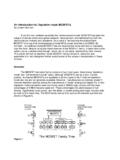
1 HDRV1SW1 LDRV1 HDRV2 TPS40140SW2 LDRV2L1CS1 VINCSRT1L2CS2 VINCSRT2 VOUT1 VOUT2 UDG 06016 ProductFolderSample &BuyTechnicalDocumentsTools &SoftwareSupport &CommunityTPS40140 SLUS660I SEPTEMBER2005 REVISEDJANUARY2015 TPS40140 dual or 2-Phase, StackableController1 Features2 Applications1 to 15 V, WithInternal5-V Regulator GraphicCards V to V InternetServers Convertsfrom15-VInputto NetworkingEquipment1 MHz TelecommunicationsEquipment dual -Outputor 2-PhaseInterleavedOperation, DC PowerDistributedSystemsStackableto 16 Phases3 Description SupportsPrebiasedOutputsThe TPS40140is a multifunctionalsynchronousbuckProgrammab leSwitchingFrequencyup tocontrollerthat can be configuredto provideeithera1 MHz/Phasesingle-output2-phasepowersupply or a power 10- A ShutdownCurrentSeveralTPS40140controller scan be stackedup to , CurrentModeControlWithForcedCurrentsever alcontrollersprovidingmultipleindependen tSharing(1)outputscanbe synchronizedin an interleaving 1- to 40-VPowerStageOperationRangepatternfor improvedinputripplecurrent.
2 PowerSharingFromDifferentInputVoltageRai ls,The TPS40140can convertfroma 15-Vinputto a(for Example,MasterFrom5 V, SlaveFrom12 V) 1 MHz. TrueRemoteSensingDifferentialAmplifierEa chphaseoperatesat a switchingfrequencyof up ProgrammableInputUndervoltageLockoutto 1 phasesin onedeviceoperate(UVLO)180 a multiple-devicestackable Resistiveor InductorDCRC urrentSensingconfiguration,the phaseshift of the slaves,relativetoa master,is programmable. Providea 6-BitDigitallyControlledOutputWhenUsedWi thTPS40120 DeviceInformation(1) 36-PinVQFNP ackagePARTNUMBERPACKAGEBODYSIZE(NOM)TPS4 0140 VQFN(36) (1) For all availablepackages,see the orderableaddendumatthe end of the datasheet.
3 (1)PatentsPendingSimplifiedSchematic1An IMPORTANTNOTICEat the end of this datasheetaddressesavailability,warranty, changes,use in safety-criticalapplications,intellectual propertymattersand SEPTEMBER2005 Applicationand Pin Configurationand Deviceand Mechanical,Packaging,and RevisionHistoryNOTE:Pagenumbersfor previousrevisionsmay differfrompagenumbersin the (June2013)to RevisionIPage AddedESDR atingstable,ESDR atingstableFeatureDescriptionsection,Dev iceFunctionalModes,Applicationand Implementationsection,PowerSupplyRecomme ndationssection,Layoutsection,Deviceand DocumentationSupportsection,andMechanica l,Packaging,and AddedR1to resistorin Figure33.
4 33 ChangesfromRevisionG (July2013)to RevisionHPage Changedmax Operatingjunctiontemperaturefrom125 to 150 ChangedswitchingfrequencyequationinSetti ngthe SwitchingFrequencyto ChangedPhaseFrequencyvs TimingResistorcurveinSettingthe SwitchingFrequencyto (September2009)to RevisionGPage Addedclarityto Addedclarityto 2005 2015,TexasInstrumentsIncorporatedProduct FolderLinks:TPS40140FB1 COMP1 ILIM1 TRK1 CSRT1CS1 PGOOD1 UVLO_CE1 CLKIO272625242322212019 DIFFOVOUTGSNSPHSELRTVSHAREGNDBP5FB212345 6789 BOOT1 HDRV1SW1 LDRV1 PGNDLDRV2 VREGSW2 HDRV2 COMP2 ILIM2 TRK2 CSRT2CS2 PGOOD2 UVLO SEPTEMBER2005 REVISEDJANUARY20155 DeviceComparisonTableDEVICEDESCRIPTIONTP S401302-phasesynchronousbuckcontrollerwi th integratedMOSFET driversTPS400904-channelmulti-phaseDC-DC controllerwith tri-stateTPS40120 Feedbackdivider,digitallycontrolled6 Pin Configurationand FunctionsRHHPACKAGEVQFN36-PINS(TOPVIEW)T he thermalpad is an FunctionsPIN(1)
5 Bootstrappedsupplyfor the high side FET driverfor PWM1,enablingthe gateof the highBOOT127 Iside FET to be drivenabovethe inputsupplyrail. Connecta capacitorfromBOOT1to SW1pin and a Schottkydiodefromthis pin to bootstrappedsupplyfor the high side FET driverfor PWM2,enablingthe gateof the highBOOT218 Iside FET to be drivenabovethe inputsupplyrail. Connecta capacitorfromBOOT2to SW2pin and a Schottkydiodefromthis pin to VREGpin. A 10- resistorshouldbe connectedbetweenVREGand BP5 and a FBP58 Iceramiccapacitorshouldbe connectedfromBP5 to synchronizingslavecontrollersto the masterCLKIO frequencyand is either6 or 8 timesCLKIO28 Othe the erroramplifier, voltageat this pin determinesthe duty cyclefor the PWM1.
6 (1)It is oftennecessaryto referto a pin or pins that are usedin CH1 shortcutnomenclatureusedis the pin namewith alowercase'x' to meaneitheror example,TRKxrefersto TRK1 2005 2015,TexasInstrumentsIncorporatedSubmitD ocumentationFeedback3 ProductFolderLinks: TPS40140 TPS40140 SLUS660I SEPTEMBER2005 Functions(continued)PIN(1) the erroramplifier, voltageat this pin determinesthe duty cyclefor the are usedto sensethe be sensedwith an externalcurrentCS131 Isenseresistoror by usingan externalR-C circuitand the inductor s DC tracesfor thesesignalsmustbe connecteddirectlyat the are usedto sensethe be sensedwith an externalcurrentCS214 Isenseresistoror by usingan externalR-C circuitand the inductor s DC tracesfor thesesignalsmustbe connecteddirectlyat the the outputvoltageof the differentialamplifieris limitedto V.
7 For remotesensing,the voltageat this pin representsthe true outputvoltagewithoutI R dropsthat resultfromhighDIFFO1 Ocurrentin the VOUTand GSNS pins mustbe connecteddirectlyat the pointof load whereregulationis tracefor this signalmustbe connecteddirectlyat the tracefor this signalmustbe connecteddirectlyat the the erroramplifierfor closedloop operation,the voltageat this pin is nominally700FB136 ImV. This pin is also monitoredfor PGOOD1and undervoltageon the erroramplifierfor closedloop operation,the voltageat this pin is nominally700FB29 ImV. This pin is also monitoredfor PGOOD2and undervoltageon Low noisegroundconnectionto the the pin shouldbe connectedto groundat the the differentialGSNS3 Iamplifieris not used,tie this pin to GNDor the high-sideN-channelMOSFET switchfor referencedto SW1and isHDRV126 Obootstrappedfor enhancementof the high side the high-sideN-channelMOSFET switchfor referencedto SW2and isHRDV219 Obootstrappedfor enhancementof the high side set the cycle-by-cyclecurrentlimit thresholdfor the ILIM1thresholdis reached.
8 The PWMpulseILIM134 Iis terminatedand the converterdeliverslimitedcurrentto the set the cycle-by-cyclecurrentlimit thresholdfor the ILIM2thresholdis reached,the PWMpulseILIM211 Iis terminatedand the converterdeliverslimitedcurrentto the the low-sidesynchronousrectifier(SR)N-channe lMOSFETfor the low-sidesynchronousrectifier(SR)N-channe lMOSFETfor open-drainoutputconnectsto a voltagevia an externalPGOOD130 OresistorPowergoodindicatorsfor open-drainoutputconnectsto a voltagevia an externalPGOOD215 OresistorPowergroundreferencefor the a high currentreturnpathfromPGND23 the sourcesof the lowerMOSFETsto this 20 A currentflowsfromthis pin.
9 In a singlecontrollerdesign,this pin shouldbe a multiPHSEL4 Ocontrollerconfiguration,a 39- k resistorstringsets the voltageon this pin determinesthe properphasingforthe the sectiononClockMaster,PHSEL,and resistorfromthis pin to groundsets the the switchednodeon is the returnfor the CH 1 a high currentreturnpathfromthe sourceof the upperMOSFETto this pin. This pin is also usedby theadaptivegatedrivecircuitsto minimizethe deadtime betweenupperand the switchednodeon is the returnfor the CH 2 a high currentreturnpathfromthe sourceof the upperMOSFETto this pin. This pin is also usedby theadaptivegatedrivecircuitsto minimizethe deadtime betweenupperand is an inputto the non-invertinginputof the pin is normallyconnectedto the soft-TRK133 Istartcapacitoror to anothervoltagethat is is an inputto the non-invertinginputof the pin is normallyconnectedto the soft-TRK212 Istartcapacitoror to anothervoltagethat is voltagedividerfromVINto this pin determinesthe inputvoltagethat and V the VREG regulatoris enabled.
10 Whenthe voltageis V or aboveCH1soft startisallowedto 2005 2015, SEPTEMBER2005 REVISEDJANUARY2015 Pin Functions(continued)PIN(1) voltagedividerfromVINto this pin determinesthe inputvoltagethat and V the VREG regulatoris enabled. Whenthe voltageis V or aboveCH2soft startisallowedto the controller5V regulatorand F ceramiccapacitorshouldbeVDD17 Iconnectedfromthis pin to the pin shouldbe connectedto the outputof the converterVOUT2 Icloseto the load the differentialamplifieris not used,leavethis pin outputof the internal5-V F ceramiccapacitorshouldbe connectedfromthis pin (unlessotherwisenoted)MINMAXUNITVDD,UVLO VDD,RT, SS ,SW2 144 InputvoltageSW1,SW2,transient< 50 ns 5 VBOOT1,BOOT2,HDRV1,HDRV2 VSW+ otherpins ATJO peratingjunctiontemperature 40150 CTstgStoragetemperature 55150 (HBM),per ANSI/ESDA/JEDECJS-001(1)