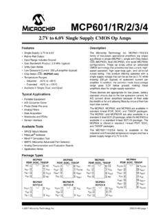
Transcription of Stand-Alone CAN Controller with SPI Interface
1 MCP2515. Stand-Alone CAN Controller with SPI Interface Features Description Implements CAN at 1 Mb/s: Microchip Technology's MCP2515 is a Stand-Alone - 0 8 byte length in the data field Controller Area Network (CAN) Controller that imple- - Standard and extended data and remote ments the CAN specification, version It is capable frames of transmitting and receiving both standard and extended data and remote frames. The MCP2515 has Receive buffers, masks and filters: two acceptance masks and six acceptance filters that - Two receive buffers with prioritized message are used to filter out unwanted messages, thereby storage reducing the host MCUs overhead. The MCP2515. - Six 29-bit filters interfaces with microcontrollers (MCUs) via an industry - Two 29-bit masks standard Serial Peripheral Interface (SPI). Data byte filtering on the first two data bytes (applies to standard data frames) Package Types Three transmit buffers with prioritizaton and abort 18-Lead PDIP/SOIC. features High-speed SPI Interface (10 MHz): TXCAN 1 18 VDD.
2 - SPI modes 0,0 and 1,1 RXCAN 2 17 RESET. One-shot mode ensures message transmission is CLKOUT/SOF 3 16 CS. attempted only one time MCP2515. TX0 RTS 4 15 SO. Clock out pin with programmable prescaler: TX1 RTS 5 14 SI. - Can be used as a clock source for other device(s) TX2 RTS 6 13 SCK. Start-of-Frame (SOF) signal is available for OSC2 7 12 INT. monitoring the SOF signal: 11. OSC1 8 RX0BF. - Can be used for time-slot-based protocols Vss 9 10 RX1BF. and/or bus diagnostics to detect early bus degredation Interrupt output pin with selectable enables Buffer Full output pins configurable as: - Interrupt output for each receive buffer 20-LEAD TSSOP. - General purpose output TXCAN 1 20 VDD. Request-to-Send (RTS) input pins individually RXCAN 2 19 RESET. configurable as: CLKOUT/SOF 3 18 CS. - Control pins to request transmission for each TX0 RTS 4 17 SO. MCP2515. transmit buffer TX1 RTS 5 16 SI. - General purpose inputs NC 6 15 NC. TX2 RTS 7 14 SCK. Low-power CMOS technology: OSC2 8 13 INT.
3 - Operates from 9 12 RX0BF. OSC1. - 5 mA active current (typical) VSS 10 11 RX1BF. - 1 A standby current (typical) (Sleep mode). Temperature ranges supported: - Industrial (I): -40 C to +85 C. - Extended (E): -40 C to +125 C. 2005 Microchip Technology Inc. Preliminary DS21801D-page 1. MCP2515. NOTES: DS21801D-page 2 Preliminary 2005 Microchip Technology Inc. MCP2515. DEVICE OVERVIEW Control Logic The MCP2515 is a Stand-Alone CAN Controller The control logic block controls the setup and operation developed to simplify applications that require of the MCP2515 by interfacing to the other blocks in interfacing with a CAN bus. A simple block diagram of order to pass information and control. the MCP2515 is shown in Figure 1-1. The device Interrupt pins are provided to allow greater system consists of three main blocks: flexibility. There is one multi-purpose interrupt pin (as 1. The CAN module, which includes the CAN well as specific interrupt pins) for each of the receive protocol engine, masks, filters, transmit and registers that can be used to indicate a valid message receive buffers.
4 Has been received and loaded into one of the receive 2. The control logic and registers that are used to buffers. Use of the specific interrupt pins is optional. configure the device and its operation. The general purpose interrupt pin, as well as status registers (accessed via the SPI Interface ), can also be 3. The SPI protocol block. used to determine when a valid message has been An example system implementation using the device is received. shown in Figure 1-2. Additionally, there are three pins available to initiate CAN Module immediate transmission of a message that has been loaded into one of the three transmit registers. Use of The CAN module handles all functions for receiving these pins is optional, as initiating message and transmitting messages on the CAN bus. Messages transmissions can also be accomplished by utilizing are transmitted by first loading the appropriate control registers, accessed via the SPI Interface . message buffer and control registers. Transmission is initiated by using control register bits via the SPI SPI Protocol Block Interface or by using the transmit enable pins.
5 Status The MCU interfaces to the device via the SPI Interface . and errors can be checked by reading the appropriate Writing to, and reading from, all registers is registers. Any message detected on the CAN bus is accomplished using standard SPI read and write checked for errors and then matched against the user- commands, in addition to specialized SPI commands. defined filters to see if it should be moved into one of the two receive buffers. FIGURE 1-1: BLOCK DIAGRAM. CAN Module RXCAN. CAN TX and RX Buffers SPI CS. Protocol Interface SCK SPI. Engine Masks and Filters Logic Bus SI. TXCAN SO. Control Logic OSC1. Timing OSC2. Generation INT. CLKOUT. RX0BF. RX1BF. TX0 RTS. Control TX1 RTS. and Interrupt TX2 RTS. Registers RESET. 2005 Microchip Technology Inc. Preliminary DS21801D-page 3. MCP2515. FIGURE 1-2: EXAMPLE SYSTEM IMPLEMENTATION. Node Node Node Controller Controller Controller SPI SPI SPI. MCP2515 MCP2515 MCP2515. TX RX TX RX TX RX. XCVR XCVR XCVR. CANH. CANL. TABLE 1-1: PINOUT DESCRIPTION.
6 PDIP/SOIC TSSOP I/O/P. Name Description Alternate Pin Function Pin # Pin # Type TXCAN 1 1 O Transmit output pin to CAN bus . RXCAN 2 2 I Receive input pin from CAN bus . CLKOUT 3 3 O Clock output pin with programmable Start-of-Frame signal prescaler TX0 RTS 4 4 I Transmit buffer TXB0 request-to-send. General purpose digital input. 100 k internal pull-up to VDD 100 k internal pull-up to VDD. TX1 RTS 5 5 I Transmit buffer TXB1 request-to-send. General purpose digital input. 100 k internal pull-up to VDD 100 k internal pull-up to VDD. TX2 RTS 6 7 I Transmit buffer TXB2 request-to-send. General purpose digital input. 100 k internal pull-up to VDD 100 k internal pull-up to VDD. OSC2 7 8 O Oscillator output . OSC1 8 9 I Oscillator input External clock input VSS 9 10 P Ground reference for logic and I/O pins . RX1BF 10 11 O Receive buffer RXB1 interrupt pin or General purpose digital output general purpose digital output RX0BF 11 12 O Receive buffer RXB0 interrupt pin or General purpose digital output general purpose digital output INT 12 13 O Interrupt output pin.
7 SCK 13 14 I Clock input pin for SPI Interface . SI 14 16 I Data input pin for SPI Interface . SO 15 17 O Data output pin for SPI Interface . CS 16 18 I Chip select input pin for SPI Interface . RESET 17 19 I Active low device reset input . VDD 18 20 P Positive supply for logic and I/O pins . NC 6,15 No internal connection Note: Type Identification: I = Input; O = Output; P = Power DS21801D-page 4 Preliminary 2005 Microchip Technology Inc. MCP2515. Transmit/Receive Buffers/Masks/Filters The MCP2515 has three transmit and two receive buffers, two acceptance masks (one for each receive buffer) and a total of six acceptance filters. Figure 1-3. shows a block diagram of these buffers and their connection to the protocol engine. FIGURE 1-3: CAN BUFFERS AND PROTOCOL ENGINE BLOCK DIAGRAM. BUFFERS Acceptance Mask RXM1. Acceptance Filter RXF2. A. A Acceptance Mask Acceptance Filter c TXB0 TXB1 TXB2 RXM0 RXF3. c c MESSAGE. MESSAGE. MESSAGE. c Acceptance Filter Acceptance Filter e TXREQ. TXREQ.
8 TXREQ. TXERR. TXERR. TXERR. e RXF0 RXF4 p MLOA. MLOA. MLOA. ABTF. ABTF. ABTF. p t Acceptance Filter Acceptance Filter t RXF1 RXF5. R R. M. X Identifier Identifier X. Message A. B B. Queue B. 0 1. Control Transmit Byte Sequencer Data Field Data Field PROTOCOL Receive REC. Error ENGINE Counter TEC. Transmit ErrPas Error BusOff Counter Transmit<7:0> Receive<7:0>. Shift<14:0>. {Transmit<5:0>, Receive<8:0>}. Comparator Protocol Finite SOF. State CRC<14:0> Machine Bit Transmit Timing Clock Logic Logic Generator TX RX. Configuration Registers 2005 Microchip Technology Inc. Preliminary DS21801D-page 5. MCP2515. CAN Protocol Engine ERROR MANAGEMENT LOGIC. The CAN protocol engine combines several functional The Error Management Logic (EML) is responsible for blocks, shown in Figure 1-4 and described below. the fault confinement of the CAN device. Its two counters, the Receive Error Counter (REC) and the PROTOCOL FINITE STATE Transmit Error Counter (TEC), are incremented and MACHINE decremented by commands from the bit stream processor.
9 Based on the values of the error counters, The heart of the engine is the Finite State Machine the CAN Controller is set into the states error-active, (FSM). The FSM is a sequencer that controls the error-passive or bus-off. sequential data stream between the TX/RX shift register, the CRC register and the bus line. The FSM BIT TIMING LOGIC. also controls the Error Management Logic (EML) and the parallel data stream between the TX/RX shift The Bit Timing Logic (BTL) monitors the bus line input registers and the buffers. The FSM ensures that the and handles the bus-related bit timing according to the processes of reception, arbitration, transmission and CAN protocol. The BTL synchronizes on a recessive- error-signaling are performed according to the CAN to-dominant bus transition at Start-of-Frame (hard syn- protocol. The automatic retransmission of messages chronization) and on any further recessive-to-dominant on the bus line is also handled by the FSM. bus line transition if the CAN Controller itself does not transmit a dominant bit (resynchronization).
10 The BTL. CYCLIC REDUNDANCY CHECK also provides programmable time segments to compensate for the propagation delay time, phase The Cyclic Redundancy Check register generates the shifts and to define the position of the sample point Cyclic Redundancy Check (CRC) code, which is within the bit time. The programming of the BTL. transmitted after either the Control Field (for messages depends on the baud rate and external physical delay with 0 data bytes) or the Data Field and is used to times. check the CRC field of incoming messages. FIGURE 1-4: CAN PROTOCOL ENGINE BLOCK DIAGRAM. RX TX. Bit Timing Logic Transmit Logic SAM. REC. Sample<2:0> Receive Error Counter TEC. StuffReg<5:0>. Transmit ErrPas Majority Error Counter Decision BusOff BusMon Comparator CRC<14:0>. Protocol FSM SOF. Comparator Shift<14:0>. (Transmit<5:0>, Receive<7:0>). Receive<7:0> Transmit<7:0>. RecData<7:0> TrmData<7:0>. Interface to Standard Buffer Rec/Trm Addr. DS21801D-page 6 Preliminary 2005 Microchip Technology Inc.
