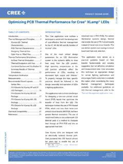
Transcription of SuperBlue™ Generation II LEDs - Cree Inc.
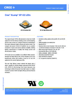
1 1 Subject to change without Low Wavelength Variation 461-465 nm at 10 mA High Performance mW (463 nm) Superior SiC Substrate Technology Excellent Chip-to-Chip Consistency High Reliability Single Wire Bond Structure Class 2 ESD RatingAPPLICATIONS Automotive Applications Dashboard Lighting Interior Lighting Toggle Switch Lighting Electronic Signs and Displays Indicator LightsSuperBlue Gen 2 LEDsData SheetC430CB230-S2100 Cree s low-current SuperBlue Generation II LEDs combine highly efficient GaN with Cree s proprietary G SiC substrate to deliver the ultimate price/performance for blue LEDs. The C430CB230-S2100 is designed for automotive applications or any application where wavelength stability and chip robustness are Chip Diagram Data Sheet: CPR3DM Rev.
2 BTop ViewBottom View200 x 200 mSiC Substratet = 250 mBacksideMetallizationGold Bond Pad114 m DiameterDie Cross SectionCathode (-)Anode (+)Mesa (junction)180 x 180 m 2008-2019 Cree, Inc. All rights reserved. The information in this document is subject to change without notice. Cree , the Cree logo and G SiC are registered trademarks, and SuperBlue is a trademark of Cree, Inc. Hysol is a registered trademark of Henkel Rev. B (201901)Cree, Silicon DriveDurham, NC 27703-8475 USATel: +1-919-313-5300 Fax: + Ratings at TA = 25 C Notes 1&3C430CB230-S2100DC Forward Current15 mAPeak Forward Current (1/10 duty cycle @ 1kHz)35 mALED Junction Temperature125 CReverse Voltage5 VOperating Temperature Range-40 C to +100 CLED Chip Storage Temperature Range (LED Chip only, not for Die Sheet Storage)-40 C to +120 CRecommended Die Sheet Storage Conditions 30 C / 85% RHElectrostatic Discharge Threshold (HBM)Note 21000 VElectrostatic Discharge Classification (MIL-STD-883E)Note 2 Class 2 Typical Electrical/Optical Characteristics at TA = 25 C, If = 10 mA Note 3 Part NumberForwardVoltage(Vf, V)Radiant Flux(P, mW)Reverse Current[I(Vr=5V), A]PeakWavelength( d, nm)
3 DominantWavelength( d, nm)Full WidthHalf Max( D, nm) SpecificationsC430CB230-S0100 DescriptionDimensionToleranceP-N Junction Area ( m 2)180 x 180 35 Top Area ( m 2)200 x 200 35 Bottom Area ( m 2)200 x 200 35 Chip Thickness ( m)250 25Au Bond Pad Diameter ( m)114 20Au Bond Pad Thickness ( m) Contact Metal Diameter ( m)114 20 Notes:1. Maximum ratings are package dependent. The above ratings were determined using a T-1 3/4 package (with Hysol OS4000 epoxy) for characterization. Ratings for other packages may differ. The forward currents (DC and Peak) are not limited by the die but by the effect of the LED junction temperature on the package.
4 The junction temperature limit of 125 C is a limit of the T-1 3/4 package; junction temperature should be characterized in a specific package to determine limitations. Assembly processing temperature must not exceed 325 C (<5 seconds).2. Product resistance to electrostatic discharge (ESD) according to the HBM is measured by simulating ESD using a rapid avalanche energy test (RAET). The RAET procedures are designed to approximate the maximum ESD ratings shown. The ESD classification of Class II is based on sample testing according to All products conform to the listed minimum and maximum specifications for electrical and optical characteristics, when assembled and operated at 10 mA within the maximum ratings shown above.
5 Efficiency decreases at higher currents. Typical values given are within the range of average values expected by the manufacturer in large quantities and are provided for information only. All measurements were made using lamps in T-1 3/4 packages (with Hysol OS4000 epoxy). Optical characteristics measured in an integrating sphere using Illuminance A. 2008-2019 Cree, Inc. All rights reserved. The information in this document is subject to change without notice. Cree , the Cree logo and G SiC are registered trademarks, and SuperBlue is a trademark of Cree, Inc. Hysol is a registered trademark of Henkel Rev.
6 B (201901)Cree, Silicon DriveDurham, NC 27703-8475 USATel: +1-919-313-5300 Fax: + CurvesThese are representative measurements for the CB230 LED product. Actual curves will vary slightly for the various radiant flux and dominant wavelength Shift vs Forward (mA)Shift (nm)Forward Current vs Forward (V)If (mA)Wavelength Shift vs Forward (mA)Shift (nm)Forward Current vs Forward (V)If (mA)Relative Intensity vs Forward Voltage010203040506070809010011012013014 01501601701800510152025If (mA)% Relative Intensity 2008-2019 Cree, Inc. All rights reserved. The information in this document is subject to change without notice. Cree , the Cree logo and G SiC are registered trademarks, and SuperBlue is a trademark of Cree, Inc.
7 Hysol is a registered trademark of Henkel Rev. B (201901)Cree, Silicon DriveDurham, NC 27703-8475 USATel: +1-919-313-5300 Fax: + PatternThis is a representative radiation pattern for the CB230 LED product. Actual patterns will vary slightly for each chip. 2008-2019 Cree, Inc. All rights reserved. The information in this document is subject to change without notice. Cree , the Cree logo and G SiC are registered trademarks, and SuperBlue is a trademark of Cree, Inc. Hysol is a registered trademark of Henkel Rev. B (201901)Cree, Silicon DriveDurham, NC 27703-8475 USATel: +1-919-313-5300 Fax: + Content Information and WarningsThis information is not intended as legal advice.
8 Consult a qualified lawyer if you are unfamiliar with the applicability of China RoHS 2 and/or California Proposition 65 to your business and RoHS 2 This green e logo is included on this product datasheet to indicate that the Cree product described herein does not include any of chemicals regulated under China RoHS 2 above permissible threshold limits. As applicable, each customer that incorporates this Cree product into its higher-level product needs to decide on the appropriate China RoHS 2 label for its higher-level product based on any other regulated content used in its product. If no other regulated content is present, this green e logo also may be used for the customer s to Management Methods for Restricted Use of Hazardous Substances in Electrical and Electronic Products, an administrative order published by the Chinese Ministry of Industry and Information Technology (MIIT) and effective as of July 1, 2016 (more commonly known as China RoHS 2 ), electronic and electrical end products (EEPs)
9 Sold into China must be marked with a logo to indicate whether or not they contain any of the chemicals regulated under China RoHS 2 ( , lead, mercury, cadmium, hexavalent chromium, polybrominated biphenyls, or polybrominated diphenyl ethers) above the permissible threshold limits. As of March 2018, the list of EEPs includes refrigerators, air conditioners, washing machines, water heaters, printers, copiers, fax machines, TV sets. monitors, microcomputers, cell phones, and telephones. This list is subject to modification by the MIIT. According to MIIT guidance, suppliers supporting the manufacture of EEPs ( , component suppliers) may but are not required to include a label on their component products.
10 However, if a component product includes one of the regulated substances, the component supplier must provide the purchaser with information in a prescribed tabular format to facilitate labeling EEPs. The table must disclose the type and location of the hazardous substances contained in the component product. If a component product that could be used in an EEP is sold separately in the market, the component product falls within the scope of China RoHs unless the final purpose is known to be out of scope. A supplier that does not directly sell products in China should nevertheless comply with China RoHS 2 if there is a possibility that its products or products incorporating its products will be sold in China.