Transcription of Supertex inc. - Microchip Technology
1 Supertex inc. DN2535. N-Channel Depletion-Mode Vertical DMOS FETs Features General Description High input impedance The Supertex DN2535 is a low threshold depletion mode Low input capacitance (normally-on) transistor utilizing an advanced vertical Fast switching speeds DMOS structure and Supertex 's well-proven silicon-gate Low on-resistance manufacturing process. This combination produces a device Free from secondary breakdown with the power handling capabilities of bipolar transistors and with the high input impedance and positive temperature Low input and output leakage coefficient inherent in MOS devices. Characteristic of all Applications MOS structures, this device is free from thermal runaway and thermally-induced secondary breakdown. Normally-on switches Solid state relays Supertex 's vertical DMOS FETs are ideally suited to a Converters wide range of switching and amplifying applications where Linear amplifiers high breakdown voltage, high input impedance, low input Constant current sources capacitance, and fast switching speeds are desired.
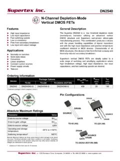
2 Power supply circuits Telecom Ordering Information Product Summary Part Number Package Option Packing RDS(ON) IDSS. BVDSX/BVDGX. DN2535N3-G TO-92 1000/Bag (max) (min). DN2535N3-G P002 350V 25 150mA. DN2535N3-G P003. DN2535N3-G P005 TO-92 2000/Reel Pin Configuration DRAIN. DN2535N3-G P013. DN2535N3-G P014. DN2535N5-G TO-220 50/Tube DRAIN. -G denotes a lead (Pb)-free / RoHS compliant package. SOURCE. Contact factory for Wafer / Die availablity. SOURCE. Devices in Wafer / Die form are lead (Pb)-free / RoHS compliant. GATE. Absolute Maximum Ratings GATE DRAIN. Parameter Value 3-Lead TO-92 3-Lead TO-220. Drain-to-source voltage BVDSX Product Marking Drain-to-gate voltage BVDGX SiDN YY = Year Sealed Gate-to-source voltage 20V 2 5 3 5 WW = Week Sealed YYWW = Green Packaging Operating and storage -55OC to +150OC Package may or may not include the following marks: Si or temperature Absolute Maximum Ratings are those values beyond which damage to the device 3-Lead TO-92.
3 May occur. Functional operation under these conditions is not implied. Continuous operation of the device at the absolute rating level may affect device reliability. All L = Lot Number voltages are referenced to device ground. YY = Year Sealed DN2535N5. LLLLLLLLL WW = Week Sealed Typical Thermal Resistance YYWW. = Green Packaging Package ja Package may or may not include the following marks: Si or TO-92 132 C/W O 3-Lead TO-220. TO-220 29 C/WO. Doc.# DSFP-DN2535. B062813. Supertex inc. DN2535. Thermal Characteristics ID ID Power Dissipation Package IDR IDRM. (continuous) (pulsed) @TC = 25OC. TO-92 120mA 500mA 120mA 500mA. TO-220 500mA 500mA 15W 500mA 500mA. Notes: ID (continuous) is limited by max rated Tj. Electrical Characteristics (T A. = 25OC unless otherwise specified). Sym Parameter Min Typ Max Units Conditions BVDSX Drain-to-source breakdown voltage 350 - - V VGS = , ID = 100 A. VGS(OFF) Gate-to-source off voltage - V VDS = 25V, ID = 10 A.
4 VGS(OFF) Change in VGS(OFF) with temperature - - mV/ C O. VDS = 25V, ID = 10 A. IGSS Gate body leakage current - - 100 nA VGS = 20V, VDS = 0V. - - 10 A VDS = Max rating, VGS = -10V. ID(OFF) Drain-to-source leakage current VDS = Max Rating, - - mA. VGS = -10V, TA = 125OC. IDSS Saturated drain-to-source current 150 - - mA VGS = 0V, VDS = 25V. RDS(ON) Static drain-to-source on-state resistance - 17 25 VGS = 0V, ID = 120mA. RDS(ON) Change in RDS(ON) with temperature - - %/ C O. VGS = 0V, ID = 120mA. GFS Forward transconductance - 325 - mmho VDS = 10V, ID = 100mA. CISS Input capacitance - 200 300 VGS = -10V, COSS Common source output capacitance - 12 30 pF VDS = 25V, CRSS Reverse transfer capacitance - f = td(ON) Turn-on delay time - - 10. tr Rise time - - 15 VDD = 25V, ns ID = 150mA, td(OFF) Turn-off delay time - - 15 RGEN = 25 , tf Fall time - - 20. VSD Diode forward voltage drop - - V VGS = -10V, ISD = 120mA.
5 Trr Reverse recovery time - 800 - ns VGS = -10V, ISD = Notes: 1. All parameters 100% tested at 25OC unless otherwise stated. (Pulse test: 300 s pulse, 2% duty cycle.). 2. All parameters sample tested. Switching Waveforms and Test Circuit 0V 90% VDD. INPUT Pulse RL. 10% Generator -10V OUTPUT. t(ON) t(OFF). RGEN. td(ON) tr td(OFF) tf VDD INPUT 10% 10%. OUTPUT. 0V 90% 90%. Doc.# DSFP-DN2535. B062813. Supertex inc. 2 DN2535. Typical Performance Curves Output Characteristics Saturation Characteristics 250. VGS = VGS = 200 0V. 0V. ID (milliamps). ID (amperes). 150. 100. 50. 0 0. 0 80 160 240 320 400 0 1 2 3 4 5. VDS (volts) VDS (volts). Transconductance vs. Drain Current Power Dissipation vs. Case Temperature 20. VDS = 10V TA = 25OC. TA = -55OC. TO-220. 25OC. GFS (seimens). PD (watts). 10. 125OC. TO-92. 0 0. 0 50 100 150 200 250 0 25 50 75 100 125 150. ID (amperes) TC (OC). Maximum Rated Safe Operating Area Thermal Response Characteristics TO-92/TO-220 (pulsed).
6 TA = 25OC TO-220 (DC). Thermal Resistance (normalized). TO-92 (DC). ID (amperes). TO-220. TC = 25OC. PD = 15W. TO-92. TC = 25OC. PD = TC = 25OC. 0. 10 100 1000 10. VDS (volts) tp (seconds). Doc.# DSFP-DN2535. B062813. Supertex inc. 3 DN2535. Typical Performance Curves (cont.). BVDSS Variation with Temperature On-Resistance vs. Drain Current 100. VGS = VGS = 0V. 80. BVDSS (normalized). RDSS(ON) (ohms). 60. 40. 20. 0. -50 0 50 100 150 0 80 160 240 320 400. Tj (OC) ID (amperes). Transfer Characteristics V(th) and RDS Variation with Temperature VDS = 10V TA = -55OC. 25OC VGS(th) (normalized) RDS(ON) @ ID = 120mA. ID (amperes). 125OC. VGS(OFF) @10 A. 0 0. -3 -2 -1 0 1 2 -50 0 50 100 150. VGS (volts) Tj (OC). Capacitance vs. Drain-to-Source Voltage Gate Drive Dynamic Characteristics 200. f = 1 MHz CISS 15. VGS = -10V. 150. 10. C (picofarads). VGS (volts). 100 5. VDS = 20V. 200pF. 0 VDS = 40V. 50. COSS -5.
7 CRSS 170pF. 0. 0 10 20 30 40 0 VDS (volts) QG (nanocoulombs). Doc.# DSFP-DN2535. B062813. Supertex inc. 4 DN2535. 3-Lead TO-92 Package Outline (N3). D. A. Seating Plane 1 2 3. L. b c e1. e Front View Side View E. E1. 1 3. 2. Bottom View Symbol A b c D E E1 e e1 L. MIN .170 .014 .014 .175 .125 .080 .095 .045 .500. Dimensions NOM - - - - - - - - - (inches). MAX .210 .022 .022 .205 .165 .105 .105 .055 .610*. JEDEC Registration TO-92. * This dimension is not specified in the JEDEC drawing. This dimension differs from the JEDEC drawing. Drawings not to scale. Supertex Doc.#: DSPD-3TO92N3, Version E041009. Doc.# DSFP-DN2535. B062813. Supertex inc. 5 DN2535. 3-Lead TO-220 Package Outline (N5). A. Seating E Plane A E. E2 A1. P. Q. H1 H1. 4 D1. D. Chamfer Optional Thermal D1 Pad 1 2 3 E1. View L. B. A2. e c A. Front View Side View View A - A. 1 2 3. L1. b2 b View B. Symbol A A1 A2 b b2 c D D1 D2 E E1 E2 e H1 L L1 Q P.
8 MIN .140 .020 .080 .015 .045 .012 ..560 .326 ..474 ..380 .270 * .230 .500 .200* .100 .139. Dimen- .100. sion NOM - - - .027 .057 - - - - - - - - - - - - BSC. (inches). MAX .190 .055 .120 ..040 .070 .024 .650 .361 ..507 .420 .350 .030 .270 .580 .250 .135 .161. JEDEC Registration TO-220, Variation AB, Issue K, April 2002. * This dimension is not specified in the JEDEC drawing. This dimension differs from the JEDEC drawing. Drawings not to scale. Supertex Doc. #: DSPD-3TO220N5, Version C041009. (The package drawing(s) in this data sheet may not reflect the most current specifications. For the latest package outline information go to ). Supertex inc. does not recommend the use of its products in life support applications, and will not knowingly sell them for use in such applications unless it receives an adequate product liability indemnification insurance agreement. Supertex inc. does not assume responsibility for use of devices described, and limits its liability to the replacement of the devices determined defective due to workmanship.
9 No responsibility is assumed for possible omissions and inaccuracies. Circuitry and specifications are subject to change without notice. For the latest product specifications refer to the Supertex inc. (website: ). 2013 Supertex inc. All rights reserved. Unauthorized use or reproduction is prohibited. Supertex inc. 1235 Bordeaux Drive, Sunnyvale, CA 94089. Doc.# DSFP-DN2535 Tel: 408-222-8888. B062813 6