Transcription of Switched Capacitor Band-Pass Filter
1 Switched Capacitor Band-Pass ObjectTheobjectofthisexperimentistodesig nandimplementafourth-orderChebyshevband- passfilter using a Switched - Capacitor realization. The specifications of thefilter are: , center frequencyfC=4kHz, 3dBbandwidthf3dB=2kHz,gainatthecenter frequencyHBP=1. The transfer function is to be realized as the product of asecond-order high-passfilter in cascade with a second-order obtain the transfer function for thefilter, see page 13 of the Filter Potpourri. Followthe example for the8thorder band-passfilter to solve for the required value ofxandBin thefrequency transformation from a low-passfilter function to a band-passfilter function.
2 Thefrequency transformation for the band-passfilter is given on page6of the Filter it to solve for the transfer you obtain the Band-Pass transfer function, use Mathcad or any math program toplot thedBgain versus frequency for the function. If you use Mathcad, be sure to use a rangevariable for the frequency that gives equal x-axis spacings on a log scale. Check to see if thecenter frequency and the 3dBbandwidth are correct. If they are correct, use Mathcad tofactor the denominator of the transfer function into the product of two second-order the factored transfer function as the product of a high-passfilter function andalow-passfilter function.
3 Realize the twofilter functions using the methods and hardwaredescribed below. The parts will be supplied by our laboratory support is from the lab manual for ECE 3042. It describes the devices available and how touse them. Other that that, it contains more information than is needed for this Switched Capacitor TheoryActivefilter design with op amps is a robust mature discipline. All of the classicalfilter typesthat were implemented in bygone eras with resistors, capacitors , and inductors may now beimplemented solely with resistors, capacitors , and op amps.
4 The accuracy of thesefilters islimitedbyonlytheprecisionofthecomponen tsandthepropertiesofthephysicalopampsemp loyed. If discrete resistors and capacitors are used, variations within the manufacturer sstated tolerance may produce unacceptable error in the design unless extremely expensivecomponents are resistors and capacitors required forfilter design may be fabricated on monolithicintegrated circuits along with the op amps but they usually require a large amount of area andare subject to temperature drift and other annoying effects such as parasitic fabricated on integrated circuits are usually restricted to values less than10 k OBJECT1while the upper limit for capacitors
5 Is approximately100 pF. Also, it is quite difficult toobtain precise values of passive components fabricated on integrated circuits. Such dedicatedanalogfilter integrated circuits are available but they are rather problem of component variation may be overcome with Switched use small integrated circuit capacitors whose terminals are Switched by a high fre-quency clock signal using MOSFET switches to simulate large values of resistance. TheMOSFETs are fabricated on the same integrated circuit while the clock may be external oralso resident on the integrated capacitorfilters are not a panacea.
6 They are digital circuits and are, therefore,subject to aliasing. The Nyquist criterion requires that the waveform be sampled at a rateat least twice its bandwidth to prevent aliasing. Normally the clock frequency is picked tobe large compared to the critical frequencies of thefilter (50to100times larger) to preventaliasing. Also, the output is a discrete rather than continuous waveform. To minimize bothof these defects it is customary to precede the digital Switched capacitorfilter with an anti-aliasing analog low-passfilter to limit the bandwidth and to follow the digitalfilter with ananalog deglitchingfilter.
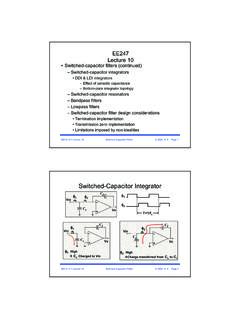
7 The break frequencies of these analogfilters are not crucial so thisuse of analogfilters at the input and output is not a major Switched Capacitor IntegratorFigure 0-1 Switched Capacitor Switched Capacitor integrator is shown in Fig. 0-1. The clock signalc(t)with frequencyfcand periodTc=1/fcis applied to both the gate input of MOSFETM1and the digital2 INVERTER. The signal applied to the gate of MOSFETM2is the complement of the , excepts for the switching transient, one MOSFET is on while the other is the clock is high MOSFETM1is on andM2is off.
8 CapacitorC1has a charge q=C1viplaced on it by the input to thefilter. If the clock frequency is large compared tothe bandwidth ofvithe input may be considered to be constant during the sampling intervalTc/2. During the next clock half cycleM1is offandM2is on which places the top node ofthe capacitorC1at the virtual ground of the op amp which causes the charge on it to betransferred into capacitorC1isi(t)= qTc=C1 Tcvi=C1fcvi(1)which means that it is equivalent to a resistorReq=1/C1fc. The output of the op amp isthen given byvo= 1 CFZt i(u)du= C1fcCFZt vi(u)du= 1 CFReqZt vi(u)du(2)which makes this circuit an integrator.
9 Integrators are the heart of the state variablefilterwhich means that any of the classicalfilters may be realized with this Switched capacitorarrangement. Other more elaborate topologies are also employed in Switched capacitorfiltersbut the circuit in Fig. 0-1 illustrates the basic charge is transferredinspurtsfromcapacitorC1to capacitorCFthis makesthe output voltage discrete rather than continuous. The voltage increments are reduced toacceptable values by picking the clock frequency to be large which is also required to preventaliasing.
10 A deglitching analog low-passfilter cascaded with the output may also be used tosmooth the output the output of the Switched Capacitor integrator depends on the ratio of two capac-itances, this can easily be fabricated on an integrated circuit. Although precise values ofcomponents are difficult to control, maintaining ratios is relatively the equivalent resistance being set asReq=1/C1fc, this makes controlling thecritical frequencies of thefilter elementary. The system clock sets the critical , suchfilters may be easily electronically a MOSFET is on the drain to source resistance is not zero but has a certain valueknow as the on-resistanceRonwhich is normally several hundred ohms.