Transcription of TSSOP8 SO8 LM2904W, LM2904AW Description LM2904, …
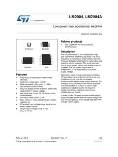
1 LM2904, LM2904A. LM2904W, LM2904AW . Datasheet Low-power dual operational amplifier Features Frequency compensation implemented internally DFN8 2x2 MiniSO8 Large DC voltage gain: 100 dB. Wide bandwidth (unity gain): MHz (temperature compensated). Very low supply current/amplifier, essentially independent of supply voltage Low input bias current: 20 nA (temperature compensated). Low input offset current: 2 nA. TSSOP8 SO8 Input common-mode voltage range includes negative rail Differential input voltage range equal to the power supply voltage Large output voltage swing 0 V to [(VCC +) V]. Description This circuit consists of two independent, high gain operational amplifiers (op amps). that have frequency compensation implemented internally. They are designed specifically for automotive and industrial control systems. The circuit operates from a single power supply over a wide range of voltages. The low power supply drain is independent of the magnitude of the power supply voltage.
2 Application areas include transducer amplifiers, DC gain blocks and all the conventional op amp circuits which can now be more easily implemented in single power supply systems. For example, these circuits can be directly supplied from the standard 5 V which is used in logic systems and easily provides the required electronic interfaces without requiring any additional power supply. Maturity status link In linear mode, the input common-mode voltage range includes ground and the Enhanced Enhanced output voltage can also swing to ground, even though operated from a single power VIO ESD. supply. LM2904. LM2904A . LM2904W . LM2904AW . Related products Dual op-amps for low- TSB572 power consumption (380 A with MHz GBP). LM2902. Quad op-amps version LM2902W. LM2904WH High temperature LM2904AH version (150 C). DS0508 - Rev 19 - April 2021 For further information contact your local STMicroelectronics sales office. LM2904, LM2904A, LM2904W, LM2904AW .
3 Schematic diagram 1 Schematic diagram Figure 1. Schematic diagram (LM2904, LM2904A). V CC. 6 A. 4 A 100 A. Q5. Q6. CC. Q2 Q3. Inverting Q7. input Q1 Q4. R SC. Non-inverting Q11. Output input Q13. Q10 Q12. Q8 Q9. 50 A. GND. Figure 2. Schematic diagram (LM2904W, LM2904AW ). A. A A. A. DS0508 - Rev 19 page 2/26. LM2904, LM2904A, LM2904W, LM2904AW . Package pin connections 2 Package pin connections Figure 3. DFN8 2x2 package pin connections (top view). Out1 1 8 Vcc+. In1- 2 7 Out2. NC (1). In1+ 3 6 In2- Vcc- 4 5 In2+. 1. The exposed pad of the DFN8 2x2 can be connected to (VCC-) or left floating. Figure 4. MiniSO8, TSSOP8 , and SO8 package pin connections (top view). Out1 1 8 Vcc+. In1- 2 - 7 Out2. In1+ 3 + - 6 In2- Vcc- 4 + 5 In2+. DS0508 - Rev 19 page 3/26. LM2904, LM2904A, LM2904W, LM2904AW . Absolute maximum ratings and operating conditions 3 Absolute maximum ratings and operating conditions Table 1. Absolute maximum ratings Symbol Parameter Value Unit VCC Supply voltage (1) 16 or 32.
4 Differential input voltage (LM2904, LM2904A) (2) 32. Vid Differential input voltage (LM2904W, LM2904AW ) (2) to VCC + V. Input voltage (LM2904, LM2904A) to 32. Vin Input voltage (LM2904W, LM2904AW ) to VCC + Output short-circuit duration (3) Infinite s 5 mA in DC or 50 mA in AC, Input current : Vin driven negative (duty cycle = 10 %, T = 1 s). Iin 5 mA in DC or 50 mA in AC, mA. Input current : Vin driven positive above VCC + V (LM2904W, LM2904AW ). (duty cycle = 10 %, T = 1 s). Input current : Vin driven positive above 32 V (5) Toper Operating free-air temperature range -40 to 125. Tstg Storage temperature range -65 to 150 C. Tj Maximum junction temperature 150. DFN8 2x2 57. MiniSO8 190. Rthja Thermal resistance junction to ambient (6). TSSOP8 120. SO8 125 C/W. MiniSO8 39. Rthjc Thermal resistance junction to case (6) TSSOP8 37. SO8 40. HBM: human body model (LM2904, LM2904A) (7) 300. HBM: human body model (LM2904W, LM2904AW ) (7) 2000 V.
5 ESD. MM: machine model (8) 200. CDM: charged device model (9) kV. 1. All voltage values, except differential voltage are with respect to network ground terminal. 2. Differential voltages are the non-inverting input terminal with respect to the inverting input terminal. 3. Short-circuits from the output to VCC can cause excessive heating if (Vcc +) > 15 V. The maximum output current is approximately 40 mA, independent of the magnitude of VCC. Destructive dissipation can result from simultaneous short-circuits on all amplifiers. 4. This input current only exists when the voltage at any of the input leads is driven negative. It is due to the collector-base junction of the input PNP transistor becoming forward-biased and thereby acting as an input diode clamp. In addition to this diode action, there is NPN parasitic action on the IC chip. This transistor action can cause the output voltages of the op amps to go to the VCC voltage level (or to ground for a large overdrive) for the time during which an input is driven negative.
6 This is not destructive and normal output is restored for input voltages above V. 5. The junction base/substrate of the input PNP transistor polarized in reverse must be protected by a resistor in series with the inputs to limit the input current to 400 A max (R = (Vin - 32 V)/400 A). 6. Short-circuits can cause excessive heating and destructive dissipation. Values are typical. DS0508 - Rev 19 page 4/26. LM2904, LM2904A, LM2904W, LM2904AW . Absolute maximum ratings and operating conditions 7. Human body model: a 100 pF capacitor is charged to the specified voltage, then discharged through a k resistor between two pins of the device. This is done for all couples of connected pin combinations while the other pins are floating. 8. Machine model: a 200 pF capacitor is charged to the specified voltage, then discharged directly between two pins of the device with no external series resistor (internal resistor < 5 ). This is done for all couples of connected pin combinations while the other pins are floating.
7 9. Charged device model: all pins and the package are charged together to the specified voltage and then discharged directly to the ground through only one pin. This is done for all pins. Table 2. Operating conditions Symbol Parameter Value Unit VCC Supply voltage 3 to 30. Common mode input voltage range Tamb = 25 C VCC- to VCC+ - V. Vicm Common mode input voltage range Tmin Tamb Tmax VCC- to VCC+ - 2. Toper Operating free-air temperature range -40 to 125 C. DS0508 - Rev 19 page 5/26. LM2904, LM2904A, LM2904W, LM2904AW . Electrical characteristics 4 Electrical characteristics Table 3. VCC + = 5 V, VCC- = ground, VO = V, RL connected to GND, Tamb = 25 C (unless otherwise specified). Symbol Parameter Min. Typ. Max. Unit Input offset voltage, Tamb = 25 C, LM2904, LM2904W (1). 2 7. Input offset voltage, Tamb = 25 C, LM2904A, LM2904AW (1) 1 2. Vio mV. Input offset voltage, Tmin Tamb Tmax, LM2904, LM2904W (1) 9. Input offset voltage, Tmin Tamb Tmax, LM2904A, LM2904AW (1) 4.
8 Vio/ T Input offset voltage drift 7 30 V/ C. Input offset current, Tamb = 25 C 2 30. Iio nA. Input offset current, Tmin Tamb Tmax 40. Iio/ T Input offset current drift 10 300 pA/ C. Input bias current, Tamb = 25 C (2). 20 150. Iib nA. Input bias current, Tmin Tamb Tmax (2) 200. Large signal voltage gain, VCC + = 15 V, RL = 2 k , 50 100. V = V to V, Tamb = 25 C. Avd V/mV. Large signal voltage gain, VCC + = 15 V, RL = 2 k , 25. V = V to V, Tmin Tamb Tmax Supply voltage rejection ratio, VCC + = 5 V to 30 V, Vicm = 0 V, 65 100. Tamb = 25 C. SVR dB. Supply voltage rejection ratio, VCC + = 5 V to 30 V, Vicm = 0 V, 65. Tmin Tamb Tmax Supply current, all amp, no load, Tamb = 25 C, VCC + = 5 V ICC mA. Supply current, all amp, no load, Tmin Tamb Tmax, VCC + = 30 V 2. Common-mode rejection ratio, VCC + = 30 V, Vicm = 0 V to V, 70 85. Tamb = 25 C. CMR dB. Common-mode rejection ratio, VCC + = 30 V, Vicm = 0 V to 28 V, 60. Tmin Tamb Tmax Isource Output short-circuit current, VCC + = 15 V, Vo = 2 V, Vid = 1 V 20 40 60.
9 MA. Output sink current, VO = 2 V, VCC + = 15 V 10 20. Isink Output sink current, VO = V, VCC + = 15 V 12 50 A. High-level output voltage (VCC + = 30 V), Tamb = 25 C, RL = 2 k 26. High-level output voltage (VCC + = 30 V), Tmin Tamb Tmax 26 27. VOH V. High-level output voltage (VCC + = 30 V), Tamb = 25 C, RL = 10 k 27. High-level output voltage (VCC + = 30 V), Tmin Tamb Tmax 27 28. Low-level output voltage (RL = 10 k ), Tamb = 25 C 5 20. VOL mV. Low-level output voltage (RL = 10 k ), Tmin Tamb Tmax 20. DS0508 - Rev 19 page 6/26. LM2904, LM2904A, LM2904W, LM2904AW . Electrical characteristics Symbol Parameter Min. Typ. Max. Unit Slew rate, VCC + = 15 V, Vin = to 3 V, RL = 2 k , CL =100 pF, unity gain, Tamb = 25 C. SR V/ s Slew rate, VCC + = 15 V, Vin = to 3 V, RL = 2 k , CL =100 pF, unity gain, Tmin Tamb Tmax Gain bandwidth product, f = 100 kHz, VCC + = 30 V, Vin = 10 mV, GBP MHz RL = 2 k , CL = 100 pF. Total harmonic distortion, f = 1 kHz, AV = 20 dB, RL = 2 k , THD %.
10 Vo = 2 Vpp, CL = 100 pF, VCC + = 30 V. en Equivalent input noise voltage, f = 1 kHz, RS = 100 , VCC + = 30 V 55 nV/ Hz VO1/VO2 Channel separation, 1 kHz f 20 kHz (3) 120 dB. 1. VO = V, 5 V < VCC + < 30 V, 0 V < Vic < (VCC +) - V. 2. The direction of the input current is out of the IC. This current is essentially constant as long as the output is not saturated, so there is no change in the loading charge on the input lines. 3. Due to the proximity of external components, ensure that the stray capacitance does not cause coupling between these external parts. This can typically be detected at higher frequencies because this type of capacitance increases. DS0508 - Rev 19 page 7/26. LM2904, LM2904A, LM2904W, LM2904AW . Electrical characteristic curves 5 Electrical characteristic curves Figure 5. Open-loop frequency response Figure 6. Large signal frequency response 140 20. 10 M . 100k . 120 F 1k +15V. - - VCC. OUTPUT S W ING (Vpp).
