Transcription of Ultralow-Noise, High-PSRR, Fast, RF, 1.5-A Low …
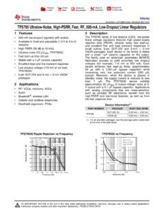
1 (Hz)10010k100k1kOutput Spectral noise Density ( V Hz)IOUT= 1 mAIOUT= AVIN= VCOUT= FCNR= F01020304050607080f (Hz)110k10M1kRipple Rejection (dB)IOUT= 1 mAIOUT= AVIN= 4 VCOUT= 10 FCNR= F10 100100k 1 MProductFolderSample &BuyTechnicalDocumentsTools &SoftwareSupport &CommunityTPS786 SLVS389M SEPTEMBER2002 REVISEDSEPTEMBER2015 TPS786 ultralow - noise , High-PSRR, fast , RF, Features3 DescriptionThe TPS786familyof low-dropout(LDO)low-power1 Availablein Fixedand Adjustable( V to V)rejectionratio(PSRR),ultralownoise,fas t start-up,OutputVersionsandexcellentline andloadtransientresponsesin HighPSRR(49 dB at 10 kHz)smalloutline, the familyis stable,with a small1- F UltralowNoise(48 VRMS, TPS78630)ceramiccapacitoron the familyusesan FastStart-UpTime(50 s)advanced,proprietaryBiCMOS fabricationprocessto StableWitha 1- F CeramicCapacitoryieldextremelylow dropoutvoltages(for example,390 mV at A).
2 Eachdeviceachievesfast start-up ExcellentLoadand Line TransientResponsetimes(approximately50 s witha F bypass VeryLow DropoutVoltage(390mV at Full Load,capacitor)whileconsumingverylowquie scentTPS78630)current(265 A, typical).Moreover,whenthe device 3 3 SONP owerPAD , 6-PinSOT223and 5-Pinis placedin standbymode,the supplycurrentisDDPAKP ackagereducedto lessthan1 A. The TPS78630exhibitsapproximately48 VRMSof outputvoltageat 3-Voutputnoisewitha F ApplicationsApplicationswithanalogcompon entsthat are noise RF: VCOs,Receivers,ADCssensitive,suchas portableRF electronics,benefit Audiofromthe highPSRR,low noisefeatures,and the fastresponsetime.
3 Bluetooth , WirelessLAN Cellularand CordlessTelephonesDeviceInformation(1) HandheldOrganizers,PDAsPARTNUMBERPACKAGE BODYSIZE(NOM)TO-263(5) (6) (8) (1) For all availablepackages,see the orderableaddendumatthe end of the FrequencyOutputSpectralNoiseDensityvsFre quency1An IMPORTANTNOTICEat the end of this datasheetaddressesavailability,warranty, changes,use in safety-criticalapplications,intellectual propertymattersand SEPTEMBER2002 Contents1 Applicationand Pin Configurationand Deviceand Mechanical,Packaging,and RevisionHistoryNOTE:Pagenumbersfor previousrevisionsmay differfrompagenumbersin the (October2010)to RevisionMPage AddedESDR atingstable,FeatureDescriptionsection,De viceFunctionalModes,ApplicationandImplem entationsection,PowerSupplyRecommendatio nssection,Layoutsection,DeviceandDocumen tationSupportsection,andMechanical,Packa ging, (August,2010)to RevisionLPage Correctedtypo in (May,2009)to RevisionKPage ReplacedtheDissipationRatingstablewith 2002 2015,TexasInstrumentsIncorporatedProduct FolderLinks.
4 TPS78612345 ENINGNDOUTNR/FB123456 GNDNR/ SEPTEMBER2002 REVISEDSEPTEMBER20155 Pin Configurationand FunctionsDCQP ackageDRBP ackage6-PinSOT-2238-SONTop ViewTop ViewKTTP ackage5-PinTO-263 Top ViewPin FunctionsPINI/ODESCRIPTIONNAMESOT-223TO- 263 SONN oise-reductionpin for externalbypasscapacitor,connectedto thisNR555 terminal,in conjunctionwith an internalresistor,createsa low-passfilter to EN terminalis an inputthat enablesor shutsdownthe is a logichigh,EN118 Ithe deviceis deviceis a logiclow, the deviceis in the , 63, TAB6 RegulatorgroundIN221, 2 IInputsupplyOUT443, 4 ORegulatoroutputCopyright 2002 2015,TexasInstrumentsIncorporatedSubmitD ocumentationFeedback3 ProductFolderLinks:TPS786 TPS786 SLVS389M SEPTEMBER2002 (unlessotherwisenoted)(1)MINMAXUNITVIN + powerdissipationSeeThermalInformationJun ctiontemperature,TJ 40150 CStoragetemperature,Tstg 65150 C(1)StressesbeyondthoselistedunderAbsolu teMaximumRatingsmay causepermanentdamageto the stressratingsonly,whichdo not implyfunctionaloperationof the deviceat theseor any otherconditionsbeyondthoseindicatedunder RecommendedOperatingConditions.
5 Exposureto absolute-maximum-ratedconditionsfor extendedperiodsmay (HBM),per ANSI/ESDA/JEDECJS-001,all pins(1) 2000V(ESD)ElectrostaticdischargeVCharged devicemodel(CDM),per JEDEC specificationJESD22-C101,all 500pins(2)(1)JEDEC documentJEP155statesthat 500-VHBM allowssafe manufacturingwith a standardESDcontrolprocess.(2)JEDEC documentJEP157statesthat 250-VCDM allowssafe manufacturingwith a (unlessotherwisenoted) 40125 C4 SubmitDocumentationFeedbackCopyright 2002 2015, SEPTEMBER2002 (3)THERMALMETRIC(1)(2)DRB(SON)DCQ(S0T-22 3)KTT(TO-263)UNIT8 PINS6 PINS5 PINSR C/WR JC(top)Junction-to-case(top) C/WR C/W C/W C/WR JC(bot)Junction-to-case(bottom) C/W(1)For moreinformationabouttraditionaland new thermalmetrics,see theSemiconductorandICPackageThermalMetri csapplicationreport,SPRA953.
6 (2)For thermalestimatesof this devicebasedon PCBcopperarea,see the TI PCBT hermalCalculator.(3)Thermaldatafor the DRB,DCQ,and DRVpackagesare derivedby thermalsimulationsbasedon JEDEC-standardmethodologyasspecifiedin the followingassumptionsare usedin the simulations:(a) i. DRB:Theexposedpadis connectedto the PCBgroundlayerthrougha 2 2 thermalvia ii. DCQ:Theexposedpadis connectedto the PCBgroundlayerthrougha 3 2 thermalvia iii. KTT:The exposedpad is connectedto the PCBgroundlayerthrougha 5 4 thermalvia array.(b) i. DRB:The top and bottomcopperlayersare assumedto havea 20%thermalconductivityof copperrepresentinga 20% ii. DCQ:Eachof topandbottomcopperlayershasa dedicatedpatternfor 20% iii.
7 KTT:The top and bottomcopperlayersare assumedto havea 20%thermalconductivityof copperrepresentinga 20%coppercoverage.(c) Thesedataweregeneratedwith only a singledeviceat the centerof a JEDEC high -K(2s2p)boardwith 3 inches 3 understandthe effectsof the copperareaon thermalperformance,see thePowerDissipationandEstimatingJunction Temperaturesectionsof this 2002 2015,TexasInstrumentsIncorporatedSubmitD ocumentationFeedback5 ProductFolderLinks:TPS786 TPS786 SLVS389M SEPTEMBER2002 (TJ= 40 C to 125 C), VEN= VIN, VIN= VOUT(nom)+ 1 V(1), IOUT= 1 mA,COUT= 10 F, and CNR= F, at 25 ,VIN(1) ,VFB(TPS78601) VDOVTPS78601(2)0 A IOUT A, VOUT+ 1 V VIN V(1)( )VOUTVOUT( )VOUTVO utputFixedVOUT0 A IOUT A, VOUT+ 1 V VIN V(1) 2%2%voltageAccuracy< 5 VFixedVOUT0 A IOUT A, VOUT+ 1 V VIN V(1) 3%3%= 5 VOutputvoltageline regulation( VOUT%/VIN)(1)VOUT+ 1 V VIN V512%/VLoadregulation( VOUT%/VOUT)0 A IOUT A7mVTPS78628 IOUT= A410580 TPS78630 IOUT= A390550 Dropoutvoltage(3)mVVIN= VOUT(nom)
8 VTPS78633 IOUT= A340510 TPS78650 IOUT= A310470 OutputcurrentlimitVOUT= 0 current0 A IOUT A260385 AShutdowncurrent(4)VEN= 0 V, V VIN AFB pin currentVFB= Af = 100 Hz, IOUT= 10 mA59f = 100 Hz, IOUT= A52 Power-supplyripplerejectionTPS78630dBf = 10 kHz,IOUT= A49f = 100 kHz,IOUT= A32 CNR= F66 CNR= F51BW = 100 Hz to 100 kHz,Outputnoisevoltage(TPS78630) VRMSIOUT= ACNR= F49 CNR= F48 CNR= F50 Time,start-up(TPS78630)RL= 2 , COUT= 1 FCNR= F75 sCNR= V VIN V VIN pin currentVEN= 0 11 (1)MinimumVIN= VOUT+ VDOor V, whicheveris TPS78650is testedat VIN= V.(2)Toleranceof externalresistorsnot includedin this specification.
9 (3)Dropoutis not measuredfor TPS78618or TPS78625becauseminimumVIN= V.(4)For adjustableversion,this appliesonly afterVINis applied;thenVENtransitionshigh to 2002 2015, (Hz)10010k100k1kOutput Spectral noise Density ( V Hz)IOUT= 1 mAIOUT= AVIN= VCOUT= 10 FCNR= (Hz)10010k100k1kOutput Spectral noise Density ( V Hz)VIN= VCOUT= 10 FIOUT= ACNR= FCNR= FCNR= FCNR= F290300310320330340350 40 25 10 5 20 35 50 65 80 95 110 125 IGND( A)TJ( C)VIN= VCOUT= 10 FIOUT= 1 mAIOUT= (Hz)10010k100k1kOutput Spectral noise Density ( V Hz)IOUT= 1 mAIOUT= AVIN= VCOUT= FCNR= F012345 40 25 10 5 20 35 50 65 80 95 110 125 VOUT(V)TJ( C)IOUT= 1 AVIN= VCOUT= 10 (V)IOUT(A)
10 VIN= 4 VCOUT= 10 FTJ= 25 SEPTEMBER2002 TPS78630 OutputVoltagevs OutputCurrentFigure2. TPS78628 OutputVoltagevs JunctionTemperatureFigure4. TPS78630 OutputSpectralNoiseDensityvsFigure3. TPS78628 GroundCurrentvs JunctionFrequencyTemperatureFigure5. TPS78630 OutputSpectralNoiseDensityvsFigure6. TPS78630 OutputSpectralNoiseDensityvsFrequencyFre quencyCopyright 2002 2015,TexasInstrumentsIncorporatedSubmitD ocumentationFeedback7 ProductFolderLinks:TPS786010203040506070 80f (Hz)110k10M1kRipple Rejection (dB)IOUT= 1 mAIOUT= AVIN= 4 VCOUT= FCNR= F10 100100k 1M01020304050607080f (Hz)110k10M1kRipple Rejection (dB)IOUT= 1 mAIOUT= AVIN= 4 VCOUT= FCNR= F10 100100k 1M01020304050607080f (Hz)110k10M1kRipple Rejection (dB)IOUT= 1 mAIOUT= AVIN= 4 VCOUT= 10 FCNR= F10 100100k 1M01020304050607080f (Hz)110k10M1kRipple Rejection (dB)IOUT= 1 mAIOUT= AVIN= 4 VCOUT= 10 FCNR= F10 100100k 1M01020304050607080 RMS Output noise ( VRMS)CNR( F) IOUT= ACOUT= 10 FBW = 100 Hz to 100 F0100200300400500600 40 25 10 5 20 35 50 65 80 95 110 125 VDO(mV)TJ( C)