Transcription of UNISONIC TECHNOLOGIES CO., LTD
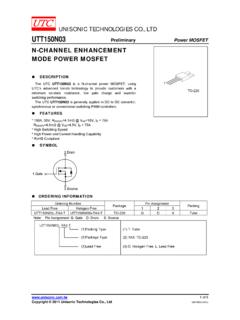
1 UNISONIC TECHNOLOGIES CO., LTD 25N10 Power MOSFET 1 of 4 Copyright 2014 UNISONIC TECHNOLOGIES Co., Ltd N-CHANNEL ENHANCEMENT MODE POWER MOSFET DESCRIPTION The UTC 25N10 is an N-channel enhancement mode power MOSFET and it uses UTC s perfect technology to provide designers with fast switching, ruggedized device design, low on-resistance and cost-effectiveness. It is generally suitable for all commercial-industrial applications and DC/DC converters requiring low voltage.
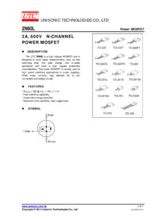
2 FEATURES * Single Drive Requirement * Low Gate Charge * RoHS Compliant SYMBOL ORDERING INFORMATION Ordering Number Package Pin Assignment Packing Lead Free Plating Halogen Free 1 2 3 25N10L-TF1-T 25N10G-TF1-T TO-220F1 G D S Tube 25N10L-TF2-T 25N10G-TF2-T TO-220F2 G D S Tube 25N10L-TF3-T 25N10G-TF3-T TO-220F G D S Tube 25N10L-TM3-T 25N10G-TM3-T TO-251 G D S Tube 25N10L-TN3-R 25N10G-TN3-R TO-252 G D S Tape Reel 25N10 Power MOSFET UNISONIC TECHNOLOGIES CO.
3 , LTD 2 of 5 MARKING INFORMATION PACKAGE MARKING TO-220F1 TO-220F2 TO-220 TO-251 TO-252 25N10 Power MOSFET UNISONIC TECHNOLOGIES CO., LTD 3 of 5 ABSOLUTE MAXIMUM RATINGS PARAMETER SYMBOLRATINGS UNIT Drain Source Voltage VDSS 100 V Gate Source Voltage VGSS 20 V Continuous Drain Current (VGS=10V)
4 TC =25 C ID 23 A TC = 100 C ID A Pulsed Drain Current (Note 2) IDM 80 A Total Power Dissipation (TC =25 C) TO-220F/TO-220F1PD 50 W TO-220F2 52 TO-251/TO-252 41 Operating Junction Temperature TJ -55 ~ +150 C Storage Temperature TSTG -55 ~ +150 C Note: 1.
5 2. Absolute maximum ratings are those values beyond which the device could be permanently damaged. Absolute maximum ratings are stress ratings only and functional device operation is not implied. Pulse width limited by max. junction temperature THERMAL DATA PARAMETER SYMBOL RATINGS UNIT Junction to Ambient TO-220F/TO-220F1TO-220F2 JA C/W TO-251/TO-252 100 Junction to Case TO-220F/TO-220F1 JC C/W TO-220F2 TO-251/TO-252 3
6 25N10 Power MOSFET UNISONIC TECHNOLOGIES CO., LTD 4 of 5 ELECTRICAL CHARACTERISTICS (TJ=25 C, unless otherwise specified) PARAMETER SYMBOL TEST CONDITIONS MIN TYP MAX UNITOFF CHARACTERISTICS Drain-Source Breakdown Voltage BVDSS VGS=0V, ID=1mA 100 V Breakdown Voltage Temperature Coefficient BVDSS/ TJReference to 25 C , ID =1mA V/ CDrain-Source Leakage Current IDSS VDS=100V.
7 VGS=0V, TJ=25 C 25 AVDS=80V, VGS =0V,TJ=150 C 100 AGate-Source Leakage Current IGSS VGS= 20V 100nAON CHARACTERISTICS Gate Threshold Voltage VGS(TH) VDS=VGS, ID=250 A 2 4 V Static Drain-Source On-Resistance (Note) RDS(ON) VGS=10V, ID=16A 80m Forward Transconductance gFS VDS=10V, ID=16A 14 S DYNAMIC PARAMETERS Input Capacitance CISS VDS =25V, VGS=0V.
8 F= 1060 1700pFOutput Capacitance COSS 270 pFReverse Transfer Capacitance CRSS 8 pFGate Resistance RG f= SWITCHING PARAMETERS Total Gate Charge (Note) QG VGS=10V, VDS=80V, ID=16A 19 30nCGate Source Charge QGS 5 nCGate Drain Charge QGD 6 nCTurn-ON Delay Time1 tD(ON) VDD=50V, ID=16A, RG= , VGS=10V, RD= 10 nsTurn-ON Rise Time tR 28 nsTurn-OFF Delay Time tD(OFF) 17 nsTurn-OFF Fall-Time tF 2 nsSOURCE- DRAIN DIODE RATINGS AND CHARACTERISTICS Drain-Source Diode Forward Voltage (Note)
9 VSD IS =16A, VGS =0V Reverse Recovery Time tRR IS =16A,VGS =0V, dI/dt=100A/ s 90 nsReverse Recovery Charge QRR 380 nCNote: Pulse Test : Pulse width 300 s, Duty cycle 2%. 25N10 Power MOSFET UNISONIC TECHNOLOGIES CO.
10 , LTD 5 of 5 TYPICAL CHARACTERISTICS Drain Current, ID( A)Drain Current, ID( A) Drain Current, ID(A)Drain Current, ID(A) UTC assumes no responsibility for equipment failures that result from using products at values thatexceed, even momentarily, rated values (such as maximum ratings, operating condition ranges, orother parameters) listed in products specifications of any and all UTC pro