Transcription of UNISONIC TECHNOLOGIES CO., LTD
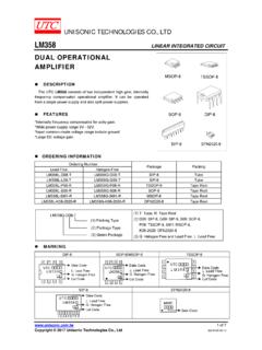
1 UNISONIC TECHNOLOGIES CO., LTD tda2030a LINEAR INTEGRATED CIRCUIT 1 of 15 Copyright 2016 UNISONIC TECHNOLOGIES Co., Ltd 18W HI-FI AUDIO AMPLIFIER AND 35W DRIVER DESCRIPTION The UTC tda2030a is a monolithic IC intended for use aslow frequency class AB amplifier. With Vs=max=44V it is particularly suited for more reliable applications without regulated supply and for 35W driver circuits using low-cost complementary pairs. The UTC tda2030a provides high output current and has very low harmonic and cross-over distortion. Further the device incorporates a short circuit protection system comprising and arrangement for automatically limiting the dissipated power so as to keep the working point of the output transistors within their safe operating area. A conventional thermal shut-down system is also included. ORDERING INFORMATION Ordering Number Lead Free Halogen Free Package Packing TDA2030AL-TA5-T TDA2030AG-TA5-T TO-220-5 Tube TDA2030AL-TB5-T TDA2030AG-TB5-T TO-220B Tube TDA2030AL-TB51-T TDA2030AG-TB51-T TO-220B1 Tube MARKING tda2030a LINEAR INTEGRATED CIRCUIT UNISONIC TECHNOLOGIES CO.
2 , ltd 2 of 14 PIN CONFIGURATION PIN NO. PIN NAME 1 Non inverting input 2 Inverting input 3 -VS 4 Output 5 +VS tda2030a LINEAR INTEGRATED CIRCUIT UNISONIC TECHNOLOGIES CO., LTD 3 of 14 ABSOLUTE MAXIMUM RATINGS (TA=25 C, unless otherwise specified) PARAMETER SYMBOLRATINGS UNIT Supply Voltage Vs 22 V Input Voltage VIN Vs V Differential Input Voltage VI(DIFF) 15 V Peak Output Current(internally limited)
3 IOUT A Total Power Dissipation at Tc=90 C PD 20 W Junction Temperature TJ -40 ~ +150 C Storage Temperature TSTG -40 ~ +150 C Note: Absolute maximum ratings are those values beyond which the device could be permanently damaged. Absolute maximum ratings are stress ratings only and functional device operation is not implied. ELECTRICAL CHARACTERISTICS (Refer to the test circuit, Vs = 16V, TA=25 C, unless otherwise specified) PARAMETER SYMBOLTEST CONDITIONS MIN TYP MAX UNITS upply Voltage VS 6 22 V Quiescent Drain Current IQ 50 80 mA Input Bias Current II(BIAS) 2 A Input Offset Voltage VI(OFF) 2 20 mV Input Offset Current II(OFF)
4 VS= 22V 20 200 nA Power Bandwidth BW POUT =15W,RL=4 100 KHz RL=4 15 18 W RL=8 10 12 W Output Power POUT d= ,Gv=26dB,f=40Hz to 15 KHz VS= 19V, RL=8 13 16 W Open Loop Voltage Gain Gvo 80 dB Closed Loop Voltage Gain Gvc f=1kHz 26 dB POUT = to 14W, RL=4 f=40Hz to 15 KHz % POUT = to 14W, RL=4 f=1kHz % Distortion d POUT = to 9W, RL=8 f=40Hz to 15 KHz % Second Order CCIF Intermodulation distortion d2 POUT =4W, RL=4 f2-f1=1 KHz % Third Order CCIF Intermodulation Distortion d3 f1=14 KHz, f2=15 KHz % Slew rate SR 8 V/ secPOUT =15W 106 dB Signal to Noise Ratio S/N RL=4 , Rg=10k , B=curve A POUT =1W 94 dB Input Noise Voltage eN B=curve A B= 22Hz to 22 KHz 2 3 10 V Input Noise Current iN B=curve A B= 22Hz to 22 KHz 50 80 200 pA Input Resistance (pin 1)
5 RIN Open loop, f=1 KHz 5 M Supply Voltage Rejection SVR RL=4 , Gv=26dB Rg=22K , f=100Hz 54 dB Thermal Shut-Down Junction Temperature TJ 145 C tda2030a LINEAR INTEGRATED CIRCUIT UNISONIC TECHNOLOGIES CO., LTD 4 of 14 APPLICATION CIRCUIT tda2030a LINEAR INTEGRATED CIRCUIT UNISONIC TECHNOLOGIES CO., LTD 5 of 14 TEST CIRCUIT UTCTDA2030A12354 VIN+Vs-VsC11 FC222 FC6100 FC4100nFC7220nFC3100nFC5220FD11N4001D11N 4001R322kR113kR41 RLR3680 SINGLE SUPPLY AMPLIFIER UTC TDA2030A12354 VIN+ F100k22 F220 F2200F1N4001R41C7220nFCR100k tda2030a LINEAR INTEGRATED CIRCUIT UNISONIC TECHNOLOGIES CO.
6 , LTD 6 of 14 TYPICAL CHARACTERISTICS 102103104105106107101-60-202060100140 PhaseGainGv(dB)180900 PhaseOpen Loop Frequency Response2428323640442448121620RL=4RL=8 Gv=26dB d= f=40 to 15kHzOutput Power vs. Supply VoltageTotal Harmonic Distortion vs. Output PowerTwo Tone CCIF Intermodulation Distortion10-110010110210-210-210-110010 1102Vs=38 VRL=8Vs=32 VRL=4f=15kHzf=1kHzGv=26dB10110210-210-11 00101102103104105 Order (2f1-f2)Order (2f2-f1) Vs=32V PoUT=4W RL=4 Gv=26dBLarge Signal Frequency Response Maximum Allowable Power Dissipation vs. Ambient Temperture10110210310430510152025 Vs= 15V RL=4 Vs= 15V RL=8-5005010015020030510152025infinite heatsinkheatsink having Rty=25 C/Wheatsink having Rth=4 C/Wheatsink having Rth=8 C/WAmbient Temperture, Ta ( C)Maximum Allowable Power Dissipation, PD(W)Frequency (kHz)Vo(Vp-p)Output Power, PoUT (W)Frequency (Hz)Supply Voltage, Vs (V)Frequency (Hz)Output Power, PoUT (W)Total Harmonic Distortion, d( % )Total Harmonic Distortion, d( % )PoUT (W) tda2030a LINEAR INTEGRATED CIRCUIT UNISONIC TECHNOLOGIES CO.
7 , LTD 7 of 14 TYPICAL PERFORMANCE OF THE CIRCUIT OF FIG. 1 PARAMETER SYMBOL TEST CONDITIONS MIN TYP MAX UNITS upply Voltage Vs 36 44 V Quiescent Drain Current IQ Vs=36V 50 mA d= , RL=4 f=40Hz to 15kHz, Vs=39V 35 d= , RL=4 f=40Hz to 15kHz, Vs=36V 28 d=10%, f=1kHz, RL=4 , Vs=39V 44 Output Power POUT d=10%,RL=4 f=1kHz,Vs=36V 35 W Voltage Gain Gv f=1kHz dB Slew Rate SR 8 V/ secPOUT=20W, f=1kHz % Total Harmonic Distortion d POUT=20W, f=40Hz to 15kHz % Input Sensitivity VIN Gv=20dB, POUT=20W.
8 F=1kHz, RL=4 890 mV RL=4 , Rg=10k B=curve A, POUT=25W 108 Signal to Noise Ratio S/N RL=4 , Rg=10k B=curve A, POUT=4W 100 dB UTC TDA2030A12354 VIN+ FR356kRL= FR256kC247FC52200F/40VC82200 F Fig. 1 Single supply high power amplifier tda2030a LINEAR INTEGRATED CIRCUIT UNISONIC TECHNOLOGIES CO., LTD 8 of 14 TYPICAL CHARACTERISTICS(Cont.) 242832343640515253545 Output Power vs. Supply VoltageOutput Power, PoUT (W)Supply Voltage, Vs (V)10-110010110-210-1100f=15kHzf=1kHz Vs=36V RL=4 Gv=20dBTotal Harmonic Distortion, d (%)Output Power, PoUT (W)Total Harmonic Distortion vs. Output Power10025040055070005101520Gv=26dBGv=20 dBInput Level, Vi (mV)Output Power, POUT (W)Output Power vs.
9 Input Level0510152008162432 Power Dssipation, PD(W)Complete AmplifierUTC TDA2030 Power Dssipation vs. Output PowerOutput Power, PoUT (W) tda2030a LINEAR INTEGRATED CIRCUIT UNISONIC TECHNOLOGIES CO., LTD 9 of 14 TYPICAL AMPLIFIER WITH SPLIT POWER SUPPLY BRIDGE AMPLIFIER WITH SPLIT POWER SUPPLY (POUT=34W, VS=16V, VS=-16V) tda2030a LINEAR INTEGRATED CIRCUIT UNISONIC TECHNOLOGIES CO., LTD 10 of 14 MULTIWAY SPEAKER SYSTEMS AND ACTIVE BOXES Multiway loudspeaker systems provide the best possible acoustic performance since each loudspeaker is specially designed and optimized to handle a limited range of frequencies.
10 Commonly, these loudspeaker systems divide the audio spectrum two or three bands. To maintain a flat frequency response over the Hi-Fi audio range the bands cobered by each loudspeaker must overlap slightly. Imbalance between the loudspeakers produces unacceptable results therefore it is important to ensure that each unit generates the correct amount of acoustic energy for its segments of the audio spectrum. In this respect it is also important to know the energy distribution of the music spectrum to determine the cutoff frequencies of the crossover filters (see Fig. 2). As an example, a 100W three-way system with crossover frequencies of 400Hz and 3 KHz would require 50W for the woofer, 35W for the midrange unit and 15W for the tweeter. Both active and passive filters can be used for crossovers but active filters cost significantly less than a good passive filter using aircored inductors and non-electrolytic capacitors.