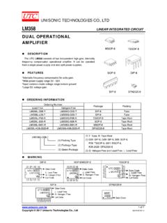
Transcription of UNISONIC TECHNOLOGIES CO., LTD
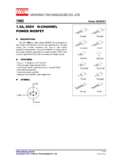
1 UNISONIC TECHNOLOGIES CO., LTD. UT2305 Power MOSFET. , 20V P-CHANNEL. POWER MOSFET. DESCRIPTION. The UTC UT2305 is P-channel enhancement mode power MOSFET, designed in serried ranks. With fast switching speed, low on-resistance, favorable stabilization. Used in commercial and industrial surface mount applications and suited for low voltage applications such as DC/DC converters. SYMBOL. ORDERING INFORMATION. Pin Assignment Ordering Number Package Packing 1 2 3 4 5 6. UT2305G-AE2-R SOT-23-3 S G D - - - Tape Reel UT2305G-AE3-R SOT-23 S G D - - - Tape Reel UT2305G-AG3-R SOT-26 D D G S D D Tape Reel Note: Pin Assignment: G: Gate D: Drain S: Source MARKING. SOT-23 / SOT-23-3 SOT-26. 1 of 4. Copyright 2015 UNISONIC TECHNOLOGIES Co.
2 , Ltd UT2305 Power MOSFET. ABSOLUTE MAXIMUM RATINGS. PARAMETER SYMBOL RATING UNITS. Drain-Source Voltage VDS - 20 V. Gate-Source Voltage VGS 12 V. Continuous Drain Current (Note 3) (TA=25 C) ID A. Pulsed Drain Current (Note 1, 2) IDM -10 A. SOT-23-3 W. Power Dissipation (TA=25 C) SOT-23 PD W. SOT-26 W. Junction Temperature TJ +150 C. Storage Temperature TSTG -55 ~ +150 C. Note: Absolute maximum ratings are those values beyond which the device could be permanently damaged. Absolute maximum ratings are stress ratings only and functional device operation is not implied. THERMAL DATA. PARAMETER SYMBOL RATING UNIT. SOT-23-3 150 C/W. Junction to Ambient (Note 3) SOT-23 JA 90 C/W. SOT-26 110 C/W. ELECTRICAL CHARACTERISTICS (TJ =25 C, unless otherwise specified).
3 PARAMETER SYMBOL TEST CONDITIONS MIN TYP MAX UNIT. OFF CHARACTERISTICS. Drain-Source Breakdown Voltage BVDSS VGS=0V, ID=-250 A -20 V. Drain-Source Leakage Current IDSS VDS=-20V, VGS=0V -1 A. Gate-Source Leakage Current IGSS VGS= 12V, VDS=0V 100 nA. Breakdown Voltage Temperature Coefficient BVDSS/ TJ Reference to 25 C, ID=-1mA V/ C. ON CHARACTERISTICS. Gate Threshold Voltage VGS(TH) VDS=VGS, ID=-250uA V. VGS=-10V, ID= 53 m . VGS= , ID= 65 m . Drain-Source On-State Resistance (Note 2) RDS(ON). VGS= , ID= 100 m . VGS= , ID= 250 m . DYNAMIC CHARACTERISTICS. Input Capacitance CISS 900 pF. Output Capacitance COSS VGS=0V, VDS=-15V, f=1 MHz 116 pF. Reverse Transfer Capacitance CRSS 120 pF. SWITCHING CHARACTERISTICS. Turn-ON Delay Time (Note 2) tD(ON) 12 ns Turn-ON Rise Time tR VDS=-15V, VGS=-10V, 36 ns Turn-OFF Delay Time tD(OFF) ID=-1A, RG=6 , RD=15 326 ns Turn-OFF Fall Time tF 200 ns Total Gate Charge (Note 2) QG 30 nC.
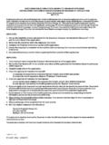
4 VDS=-16V, VGS= , Gate-Source Charge QGS 5 nC. ID= Gate-Drain Charge QGD nC. SOURCE- DRAIN DIODE RATINGS AND CHARACTERISTICS. Drain-Source Diode Forward Voltage(Note2) VSD VGS=0V, IS= V. Reverse Recovery Time trr VGS=0V, IS= , ns Reverse Recovery Charge QRR dI/dt=100A/ s 22 nC. Notes: 1. Pulse width limited by TJ(MAX). 2. Pulse width 300 s, duty cycle 2%. 3. Surface mounted on 1 in2 copper pad of FR4 board; 270 C/W when mounted on min. UNISONIC TECHNOLOGIES CO., LTD 2 of 4. UT2305 Power MOSFET. TYPICAL CHARACTERISTICS. Drain Current,-ID (A). Drain Current,-ID (A). Typical Capacitance Characteristics Gate Charge Characteristics 12 10000. f= ID= Gate to Source Voltage,-VGS (V). 10. VDS=-16V. 8 1000 CISS. C (pF). 6.
5 COSS. 4 100 CRSS. 2. 0 10. 0 5 10 15 20 25 1 5 9 13 17 21 25 29. Total Gate Charge,QG (nC) Drain-to-Source Voltage,-VDS (V). UNISONIC TECHNOLOGIES CO., LTD 3 of 4. UT2305 Power MOSFET. TYPICAL CHARACTERISTICS(Cont.). UTC assumes no responsibility for equipment failures that result from using products at values that exceed, even momentarily, rated values (such as maximum ratings, operating condition ranges, or other parameters) listed in products specifications of any and all UTC products described or contained herein. UTC products are not designed for use in life support appliances, devices or systems where malfunction of these products can be reasonably expected to result in personal injury. Reproduction in whole or in part is prohibited without the prior written consent of the copyright owner.
6 The information presented in this document does not form part of any quotation or contract, is believed to be accurate and reliable and may be changed without notice. UNISONIC TECHNOLOGIES CO., LTD 4 of 4.