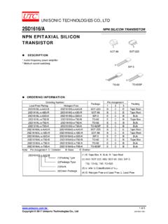
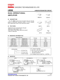
Transcription of UNISONIC TECHNOLOGIES CO., LTD
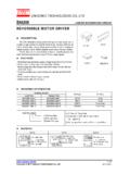
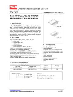
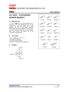
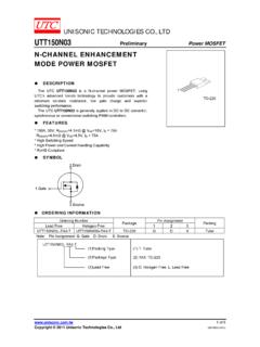
1 UNISONIC TECHNOLOGIES CO., LTD UT4392 Power MOSFET 1 of 5 Copyright 2015 UNISONIC TECHNOLOGIES Co., Ltd QW-R502-312-C 30V N-CHANNEL POWER MOSFET DESCRIPTION The UT4392 uses UTC advanced technology to provide excellent RDS(ON), low gate charge and operation with low gate voltages. This device is suitable for being used in such applications:high-Side DC/DC Conversion, notebook and sever. FEATURES * VDS(V)=30V * ID= A (VGS=10V) * High Density Cell Design for Ultra Low On-resistance * RDS(ON)< @VGS=10V * RDS(ON)< SYMBOL DGSDDDSS ORDERING INFORMATION Ordering Number Package Pin Assignment Packing 1234567 8 UT4392G-S08-R SOP-8 SSSGDDD D Tape ReelNote: Pin Assignment: G: Gate D: Drain S.
2 Source UT4392 Power MOSFET UNISONIC TECHNOLOGIES CO., LTD 2 of 4 MARKING UT4392 Power MOSFET UNISONIC TECHNOLOGIES CO., LTD 3 of 4 ABSOLUTE MAXIMUM RATINGS (TA =25 C, unless otherwise specified.)
3 PARAMETER SYMBOL RATINGS UNIT Drain-Source Voltage VDSS 30 V Gate-Source Voltage VGSS 20 V Continuous Drain Current ID A
4 Pulsed Drain Current IDM 50 A Power Dissipation(TA =25 C) PD W Junction Temperature TJ +150 C Storage Temperature TSTG -55 ~ +150 C Note: Absolute maximum ratings are those values beyond which the device could be permanently damaged.
5 Absolute maximum ratings are stress ratings only and functional device operation is not implied. THERMAL DATA PARAMETER SYMBOL MIN TYP MAX UNIT Junction to Ambient (PCB mounted) JA 50 C/W Junction to Case JC 25 C/W Notes: 1. Pulse width limited by the Maximum junction temperature. 2. Surface Mounted on FR4 Board, t 10 sec. ELECTRICAL CHARACTERISTICS (TA =25 C, unless otherwise specified.)
6 PARAMETER SYMBOLTEST CONDITIONS MIN TYP MAX UNITOFF CHARACTERISTICS Drain-Source Breakdown Voltage BVDSS VGS =0 V, ID =250 A 30 V Drain-Source Leakage Current IDSS VDS =24 V, VGS =0 V AGate-Source Leakage Current IGSS VGS = 20 V, VDS=0 V 100 nAON CHARACTERISTICS Gate-Threshold Voltage VGS(TH) VDS =VGS, IDS =250 A 1 3 V On State Drain Current (Note 1) ID(ON) VDS 5V, VGS = 10V 30 A Static Drain-Source On-Resistance(Note 1) RDS(ON) VGS =10 V, ID = A 9 m VGS = V, ID =10 A 13 m DYNAMIC PARAMETERS Input Capacitance CISS VDS =15 V, VGS =0 V, f= , (Note 2)
7 2134 pFOutput Capacitance COSS 343 pFReverse Transfer Capacitance CRSS 134 pFSWITCHING PARAMETERS Total Gate Charge QG VDS =15V, VGS =10 V, ID = , (Note 2)
8 26 nCGate Source Charge QGS 6 nCGate Drain Charge QGD 5 nCTurn-ON Delay Time tD(ON) VDD=15V,ID=1 A,VGEN=10 V RG=6 , RL=15 , (Note 3) 17 nsTurn-ON Rise Time tR nsTurn-OFF Delay Time tD(OFF)
9 40 nsTurn-OFF Fall-Time tF 6 nsSOURCE- DRAIN DIODE RATINGS AND CHARACTERISTICS Diode Forward Voltage VSD IS = A, VGS =0V Maximum Body-Diode Continuous Current IS (Note 4,5) Notes: 1.
10 Pulse Test: PW 300 S, Duty Cycle 2% 2. For DESIGN AID ONLY, not subject to production testing. 3. Switching time is essentially independent of operating temperature. 4. Pulse width limited by the Maximum junction temperature. 5. Surface Mounted on FR4 Board, t 10 sec. UT4392 Power MOSFET UNISONIC TECHNOLOGIES CO., LTD 4 of 4 TYPICAL CHARACTERISTICS Continuous Current vs.