Transcription of UNISONIC TECHNOLOGIES CO., LTD
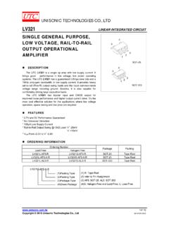
1 UNISONIC TECHNOLOGIES CO., LTD UT3401 Power MOSFET 1 of 5 Copyright 2020 UNISONIC TECHNOLOGIES Co., Ltd P-CHANNEL ENHANCEMENT MODE DESCRIPTION The UTC UT3401 is P-channel enhancement mode Power MOSFET, designed with high density cell, with fast switching speed, low on-resistance, excellent thermal and electrical capabilities and operation with low gate voltages. This device is suitable for use as a load switch or in PWM applications. SYMBOL SOT-23(EIAJ SC-59)213 ORDERING INFORMATION Ordering Number Package Pin Assignment Packing Lead Free Halogen Free 1 2 3 UT3401L-AE3-R UT3401G-AE3-R SOT-23 G S D Tape Reel Note: Pin Assignment: G: Gate S: Source D: Drain (1) R: Tape Reel(2) AE3: SOT-23(3) G: Halogen Free and Lead Free, L: Lead FreeUT3401G-AE3-R(1)Packing Type(2)Package Type(3)Green Package MARKING 34AL: Lead FreeG: Halogen Free UT3401 Power MOSFET UNISONIC TECHNOLOGIES CO.
2 , LTD 2 of 5 ABSOLUTE MAXIMUM RATINGS (TA=25 C, unless otherwise specified) PARAMETER SYMBOL RATINGS UNIT Drain-Source Voltage VDSS -30 V Gate-Source Voltage VGSS 12 V Continuous Drain Current (Note 1) ID A Pulsed Drain Current (Note 2) IDM -30 A Power Dissipation (Note 1) PD W Junction Temperature TJ +150 C Storage Temperature TSTG -55 ~ +150 C Note: Absolute maximum ratings are those values beyond which the device could be permanently damaged. Absolute maximum ratings are stress ratings only and functional device operation is not implied. THERMAL DATA PARAMETER SYMBOL RATINGS UNIT Junction-to-Ambient JA 100 C/W Notes: Surface mounted on 1 in2 copper pad of FR4 board with 2oz.
3 Copper, in a still air environment with TA=25 C. ELECTRICAL CHARACTERISTICS (TA=25 C, unless otherwise specified) PARAMETER SYMBOL TEST CONDITIONS MIN TYP MAX UNIT OFF CHARACTERISTICS Drain-Source Breakdown Voltage BVDSS ID=-250 A, VGS=0V -30 V Drain-Source Leakage Current IDSS VDS=-24V, VGS=0V -1 A Gate-Source Leakage Current IGSS VDS=0V, VGS= 12V 100 nA ON CHARACTERISTICS Gate Threshold Voltage VGS(TH) VDS=VGS, ID=-250 A -1 V Drain-Source On-State Resistance (Note 2) RDS(ON) VGS=-10V, ID= 42 50 m VGS= , ID=-4A 53 65 m VGS= , ID=-1A 80 120 m DYNAMIC PARAMETERS Input Capacitance CISS VGS =0V, VDS =-15V, f=1 MHz 875 pF Output Capacitance COSS 125 pF Reverse Transfer Capacitance CRSS 100 pF SWITCHING PARAMETERS Total Gate Charge (Note 2) QG VGS= , VDS=-15V, ID=-4A nC Gate-Source Charge QGS 2 nC Gate-Drain Charge QGD nC Turn-ON Delay Time (Note 2) tD(ON) VGS=-10V, VDS=-15V RL= , RG =6 ns Turn-ON Rise Time tR 16 ns Turn-OFF Delay Time tD(OFF) 38 ns Turn-OFF Fall Time tF 24 ns SOURCE- DRAIN DIODE RATINGS AND CHARACTERISTICS Maximum Continuous Drain-Source Diode Forward Current IS A Drain-Source Diode Forward Voltage (Note2)
4 VSD VDS=0V, IS=-1A -1 V Reverse Recovery Time trr IF=-4A, dI/dt=100A/ s ns Reverse Recovery Charge Qrr nC Notes: 1. Repetitive Rating : Pulse width limited by maximum junction temperature. 2. Pulse width 300 s, duty cycle 2%. 3. Surface mounted on 1 in2 copper pad of FR4 board with 2oz. Copper, in a still air environment with TA=25 C. UT3401 Power MOSFET UNISONIC TECHNOLOGIES CO., LTD 3 of 5 TYPICAL CHARACTERISTICS Drain Current, -ID (A)Drain-Source Voltage, -VDS (V)Drain-Source On-Resistance vs.
5 Gate-Source VoltageGate-Source Voltage, -VGS (V)Gate Charge CharacteristicsTotal Gate Charge, QG (nC)024612108 Drain-Source On-Resistance vs. Junction TemperatureJunction Temperature, TJ ( C)Drain-Source On-Resistance, RDS(ON) (m )Gate-Source Voltage, -VGS (V)Drain-Source On-Resistance, RDS(ON) (m )Breakdown Voltage vs. Junction TemperatureDrain-Source Breakdown VoltageNormalizedJunction Temperature, TJ ( C)Drain Current vs. Drain-Source VoltageVGS=-4~-10 testVDS=-15 VVGS=-10 VID= , ID=-1 AID= Voltage, -VDS (V)Capacitance, C (pF)Capacitance test-3V255075100125150255075100125150ID= , ID=-4 AVGS=-10V, ID= UT3401 Power MOSFET UNISONIC TECHNOLOGIES CO.
6 , LTD 4 of 5 TYPICAL CHARACTERISTICS (Cont.) Gate Threshold Voltage vs. Junction TemperatureJunction Temperature, TJ ( C)Source Current vs. Source-Drain VoltageSource-Drain Voltage, -VSD (V)Drain Current vs. Gate-Source VoltageGate-Source Voltage, -VGS (V)Drain Current, -ID (A)Gate Threshold Voltage, -VGS(TH) (V)Source Current, -IS (A)Drain Current, -ID (A)Drain-Source On-Resistance, RDS(ON) (m )25 CTA=150 CDrain-Source On-Resistance vs. Drain CurrentTA=25 CPulsedTA=25 CPulsedDrain Current vs. Junction TemperatureJunction Temperature, TJ ( C)Drain Current, -ID (A)ID= Dissipation vs. Junction TemperatureJunction Temperature, TJ ( C)Power Dissipation, PD (W) UT3401 Power MOSFET UNISONIC TECHNOLOGIES CO.
7 , LTD 5 of 5 TYPICAL CHARACTERISTICS (Cont.) Drain-Source Voltage, -VDS (V)Drain Current, -ID (A)Safe Operating AreaDCMAXSOT-23 Operation in this area is limited by RDS(ON)TA=25 CTJ=125 CSingle UTC assumes no responsibility for equipment failures that result from using products at values that exceed, even momentarily, rated values (such as maximum ratings, operating condition ranges, or other parameters) listed in products specifications of any and all UTC products described or contained herein. UTC products are not designed for use in life support appliances, devices or systems where malfunction of these products can be reasonably expected to result in personal injury.
8 Reproduction in whole or in part is prohibited without the prior written consent of the copyright owner. UTC reserves the right to make changes to information published in this document, including without limitation specifications and product descriptions, at any time and without notice. This document supersedes and replaces all information supplied prior to the publication hereof.