Transcription of UNISONIC TECHNOLOGIES CO., LTD
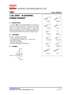
1 UNISONIC TECHNOLOGIES CO., LTD U2429 CMOS IC 1 of 7 Copyright 2019 UNISONIC TECHNOLOGIES Co., Ltd SERIAL DATA CONTROL DUAL ELECTRONIC VOLUME DESCRIPTION The UTC U2429 is a dual channel electronic volume controlled with 2-wire serial data. The built-in reference circuit can compose of an electronic volume with less external parts. FEATURES * Built-in reference circuit * Control with serial data Volume 0 ~ -83dB (1dB/step), - (Independent control is allowed in each channel) * Low noise and low distortion VNO = 5 Vrms (ATT = - ) THD = Typ. (V0 = ) ORDERING INFORMATION Ordering Number Lead Free Halogen Free Package Packing U2429L-D08-T U2429G-D08-T DIP-8 Tube U2429L-S08-R U2429G-S08-R SOP-8 Tape Reel MARKING DIP-8 SOP-8 U2429 CMOS IC UNISONIC TECHNOLOGIES CO.
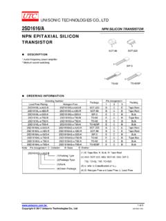
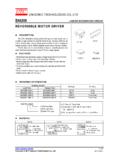
2 , LTD 2 of 7 PIN CONFIGURATION PIN DESCRIPTION PIN NO PIN NAME DESCRIPTION 1 VIN 1 1-ch input pin 2 VOUT1 1-ch output pin 3 GND Ground pin 4 DATA Control data input pin. Inputs data in synchronization with clock. 5 CLOCK Clock input pin for transferring serial data. 6 VCC Power supply pin. Stabilize the pin with decoupling capacitor. 7 VOUT2 2-ch output pin 8 VIN2 1-ch input pin BLOCK DIAGRAM U2429 CMOS IC UNISONIC TECHNOLOGIES CO., LTD 3 of 7 ABSOLUTE MAXIMUM RATING PARAMETER SYMBOL RATINGS UNIT Supply Voltage VCC.
3 VDD V SOP-8 440 mW Power Dissipation DIP-8 PD 625 mW Junction Temperature TJ 125 C Operating Temperature TOPR -20 ~ +85 C Storage Temperature TSTG -40 ~ +150 C Note: Absolute maximum ratings are those values beyond which the device could be permanently damaged. Absolute maximum ratings are stress ratings only and functional device operation is not implied. RECOMMENDED OPERATING CONDITIONS PARAMETER SYMBOL RATINGS UNIT Supply voltage range VCC ~ V Rated supply voltage VCC 5 V ELECTRICAL CHARACTERISTICS (VCC = 5V, TA= 25 C, unless otherwise noted)
4 PARAMETER SYMBOL TEST CONDITIONS MIN TYP MAX UNITC ircuit current ICC 8 16 mA Maximum attenuation ATT ATT=- -90 -80 dB Attenuation error ATT ATT=0 0 dB Maximum input voltage VIM THD=1%, ATT=-6dB VrmsMaximum output voltage VOM THD=1% VrmsVNO1 ATT=0, Rg=0 4 10 VrmsOutput noise voltage VNO2 ATT=- , Rg=0 5 10 VrmsTotal harmonic distortion THD f=1kHz, VO=.
5 ATT=0 % Channel separation CS f=1kHz -80 -70 dB DC CHARACTERISTICS OF DIGITAL BLOCK PARAMETER SYMBOLTEST CONDITIONS MIN TYP MAX UNIT"L" level input voltage VIL 0 VCCV "H" level input voltage VIH Data, clock pin VCC VCC V "L" level input current IIL VI=0 -10 10 A "H" level input current IIH VI=5V Data, clock pin 10 A AC CHARACTERISTICS OF DIGITAL BLOCK PARAMETER SYMBOLTEST CONDITIONS MINTYP MAX UNITC ycle time of clock tcr VDD=5V 4 s Pulse width of clock ("H" level) tWHC VDD=5V s Pulse width of clock ("L" level)
6 TWLC VDD=5V s Clock rising time tr VDD=5V s Clock falling time tf VDD=5V s Data setup time tSD VDD=5V s Data hold time tHD VDD=5V s Note: UTC products on power start, DATA conversion or IC first start are all without delay time.
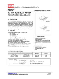
7 When DATA reading is completed, the output immediately respond. U2429 CMOS IC UNISONIC TECHNOLOGIES CO., LTD 4 of 7 RELATIONSHIP BETWEEN DATA AND CLOCK CLOCKDATAD0D1D2D3 Reads data signal at the rising edge of clock signal SYSTEM CONFIGURATION U2429 CMOS IC UNISONIC TECHNOLOGIES CO., LTD 5 of 7 CLOCK AND DATA TIMING DATA INPUT FORMAT U2429 CMOS IC UNISONIC TECHNOLOGIES CO., LTD 6 of 7 VOLUME CODE ATT1 D2 D3 D4 D5 D6 0dB H L H L H -4dB L L H L H -8dB H H L L H -12dB L H L L H -16dB H L L L H -20dB L L L L H -24dB H H H H L -28dB L H H H L -32dB H L H H L -36dB L L H H
8 L -40dB H H L H L -44dB L H L H L -48dB H L L H L -52dB L L L H L -56dB H H H L L -60dB L H H L L -64dB H L H L L -68dB L L H L L -72dB H H L L L -76dB L H L L L -80dB H L L L L L L L L L ATT2 D7 D8 0dB H H -1dB L H -2dB H L -3dB L L U2429 CMOS IC UNISONIC TECHNOLOGIES CO.
9 , LTD 7 of 7 APPLICATION EXAMPKE UTC assumes no responsibility for equipment failures that result from using products at values that exceed, even momentarily, rated values (such as maximum ratings, operating condition ranges, or other parameters) listed in products specifications of any and all UTC products described or contained herein . UTC products are not designed for use in life support appliances, devices or systems where malfunction of these products can be reasonably expected to result in personal injury. Reproduction in whole or in part is prohibited without the prior written consent of the copyright owner. UTC reserves the right to make changes to information published in this document, including without limitation specifications and product descriptions, at any time and without notice.
10 This document supersedes and replaces all information supplied prior to the publication hereof.
![[Ref. Table R602.3.5] [Ref. Tables R502.5(1) and R502.5(2 ...](/cache/preview/2/7/1/b/a/7/f/1/thumb-271ba7f161daa80f212379f2aed9ba5f.jpg)