Transcription of UNISONIC TECHNOLOGIES CO., LTD
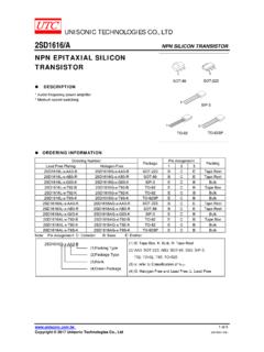
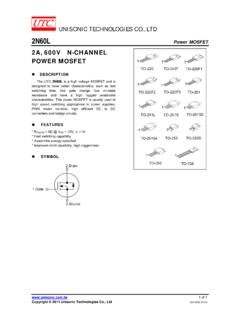
1 UNISONIC TECHNOLOGIES CO., LTD 11N90 Power MOSFET 1 of 7 Copyright 2017 UNISONIC TECHNOLOGIES Co., Ltd 11A, 900V N-CHANNEL POWER MOSFET DESCRIPTION The UTC 11N90 is a N-channel enhancement mode Power FET using UTC s advanced technology to provide customers with planar stripe and DMOS technology. This technology specializes in allowing a minimum on-state resistance and superior switching performance. It also can withstand high energy pulse in the avalanche and commutation mode. The UTC 11N90 is universally applied in high efficiency switch mode power supply, FEATURES * RDS(on) < @ VGS = 10V, ID = * High switching speed * Improved dv/dt capability * 100% avalanche tested SYMBOL ORDERING INFORMATION Ordering Number Pin Assignment Lead Free Halogen Free Package 1 2 3 Packing 11N90L-TA3-T 11N90G-TA3-T TO-220 G D S Tube 11N90L-TF1-T 11N90G-TF1-T TO-220F1 G D S Tube 11N90L-TF2-T 11N90G-TF2-T TO-220F2 G D S Tube 11N90L-T3P-T 11N90G-T3P-T TO-3P G D S Tube
2 11N90L-T3N-T 11N90G-T3N-T TO-3PN G D S Tube 11N90L-T47-T 11N90G-T47-T TO-247 G D S Tube Note: Pin Assignment: G: Gate D: Drain S: Source 11N90 Power MOSFET UNISONIC TECHNOLOGIES CO., LTD 2 of 7 MARKING 11N90 Power MOSFET UNISONIC TECHNOLOGIES CO.
3 , LTD 3 of 7 ABSOLUTE MAXIMUM RATINGS(TC=25 C, unless otherwise specified) PARAMETER SYMBOL RATINGS UNIT Drain-Source Voltage VDSS 900 V Gate-Source Voltage VGSS 30 V Continuous ID 11 A Drain Current Pulsed (Note 1) IDM 44 A Avalanche Energy Single Pulsed (Note 2)EAS 1000 mJ Peak Diode Recovery dv/dt (Note 3)
4 Dv/dt V/ns TO-220 160 W TO-220F1/TO-220F2 50 W TO-3P/TO-3PN 215 W Power Dissipation TO-247 PD 190 W Junction Temperature TJ +150 C Storage Temperature TSTG -55 ~ +150 C Note: Absolute maximum ratings are those values beyond which the device could be permanently damaged.
5 Absolute maximum ratings are stress ratings only and functional device operation is not implied. THERMAL CHARACTERISTICS PARAMETER SYMBOL RATINGS UNIT TO-220/TO-220F1 TO-220F2 C/W TO-3P/TO-3PN 40 C/W Junction to Ambient TO-247 JA 50 C/W TO-220 C/W TO-220F1/TO-220F2
6 C/W TO-3P/TO-3PN C/W Junction to Case TO-247 JC C/W 11N90 Power MOSFET UNISONIC TECHNOLOGIES CO., LTD 4 of 7 ELECTRICAL CHARACTERISTICS (TC=25 C, unless otherwise noted) PARAMETER SYMBOL TEST CONDITIONS MIN TYP MAX UNITOFF CHARACTERISTICS Drain-Source Breakdown Voltage BVDSS ID=250 A, VGS=0V 900 VBreakdown Voltage Temperature Coefficient BVDSS /TJID=250 A, Referenced to 25 C V/ CVDS=900V, VGS=0V 10 Drain-Source Leakage Current IDSS VDS=720V, TC=125 C 100 AForward VGS=+30V.
7 VDS=0V 100nAGate- Source Leakage Current Reverse IGSS VGS=-30V, VDS=0V -100 nAON CHARACTERISTICS Gate Threshold Voltage VGS(TH) VDS=VGS, ID=250 A Drain-Source On-State Resistance RDS(ON) VGS=10V, ID= DYNAMIC PARAMETERS Input Capacitance CISS 980 1380 pFOutput Capacitance COSS 170 280pFReverse Transfer Capacitance CRSS VGS=0V, VDS=25V.
8 F= 18 25pFSWITCHING PARAMETERS Total Gate Charge QG 60 80nCGate to Source Charge QGS 14 nCGate to Drain Charge QGD VGS=10V, VDS=50V, ID= (Note 4, 5) 22 nCTurn-ON Delay Time tD(ON) 125 140nsRise Time tR 260 320nsTurn-OFF Delay Time tD(OFF) 340 380nsFall-Time tF VDD=30V, ID= , RG=25 (Note 4, 5)
9 220 270nsSOURCE- DRAIN DIODE RATINGS AND CHARACTERISTICS Maximum Body-Diode Continuous Current IS 11 AMaximum Body-Diode Pulsed Current (Note1) ISM 44 ADrain-Source Diode Forward Voltage (Note 4) VSD IS=11A, VGS=0V : 1. Repetitive Rating: Pulse width limited by maximum junction temperature. 2. L = 15mH, IAS = 11A, VDD = 50V, RG = 25 , Starting TJ = 25 C 3. ISD , di/dt 200A/ s, VDD BVDSS, Starting TJ = 25 C 4. Pulse Test: Pulse width 300 s, Duty cycle 2% 5. Essentially independent of operating temperature 11N90 Power MOSFET UNISONIC TECHNOLOGIES CO.
10 , LTD 5 of 7 TEST CIRCUITS AND WAVEFORMS 50k 300nFDUTVDS10V12 VChargeQGSQGDQGGate Charge Test CircuitGate Charge WaveformsVGSVGS200nFSame Type as DUT3mA 10 VtPRGDUTLVDSIDVDDU nclamped Inductive Switching Test CircuittPVDDIASBVDSSID(t)VDS(t)TimeEAS=2 1 LIAS2 BVDSSBVDSS-VDDU nclamped Inductive Switching Waveforms 11N90 Power MOSFET UNISONIC TECHNOLOGIES CO., LTD 6 of 7 TEST CIRCUITS AND WAVEFORMS VDS+-DUTRGdv/dt controlled by RGISD controlled by pulse periodVDDPeak Diode Recovery dv/dt Test Circuit & WaveformsSame Type as DUTISDVGSLVGS(Driver)ISD(DUT)VDS(DUT)D=G ate Pulse WidthGate Pulse Period10 Vdi/dtBody Diode Reverse CurrentIRMBody Diode Recovery dv/dtVDDVSDBody Diode Forward Voltage DropIFM, Body Diode Forward CurrentDriver11N90 Power MOSFET UNISONIC TECHNOLOGIES CO.