Transcription of UNISONIC TECHNOLOGIES CO., LTD
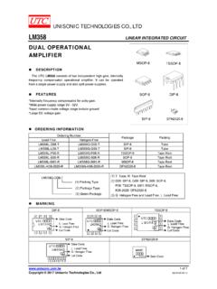
1 UNISONIC TECHNOLOGIES CO., LTD TL1451 LINEAR INTEGRATED CIRCUIT 1 of 14 Copyright 2015 UNISONIC TECHNOLOGIES Co., Ltd DUAL PULSE-WIDTH-MODULATION CONTROL CIRCUITS DESCRIPTION The UTC TL1451 incorporates on a single monolithic chip all the functions required in the construction of two pulse-width-modulation (PWM) control circuits. Designed primarily for power supply control, the UTC TL1451 contains an on-chip regulator, two error amplifiers, an adjustable oscillator, two dead-time comparators, undervoltage lockout circuitry, and dual common emitter output transistor circuits. FEATURES *Complete PWM power control circuitry *Completely synchronized operation *Internal undervoltage lockout protection *Wide supply voltage range *Internal Short-Circuit protection *Oscillator frequency 500kHz max *Variable dead time provides control over total range *Internal regulator provides a stable reference supply DIP-16 SOP-16 TSSOP-16 ORDERING INFORMATION Ordering Number Lead Free Halogen Free Package Packing TL1451L-D16-T TL1451G-D16-T DIP-16 Tube - TL1451G-P16-R TSSOP-16 Tape Reel - TL1451G-S16-R
2 SOP-16 Tape Reel MARKING DIP-16 SOP-16 / TSSOP-16 TL1451 LINEAR INTEGRATED CIRCUIT UNISONIC TECHNOLOGIES CO., LTD 2 of 14 PIN CONFIGURATION CTRT1 IN+1 IN-1 FEEDBACK1 DTC1 OUTGNDVCC2 OUT2 DTC2 IN-SCPREF2 IN+2 FEEDBACKERROR AMPLIFIER 1 ERROR AMPLIFIER 212345678910111213141516 BLOCK DIAGRAM TL1451 LINEAR INTEGRATED CIRCUIT UNISONIC TECHNOLOGIES CO., LTD 3 of 14 ABSOLUTE MAXIMUM RATINGS (TA=25 C, unless otherwise specified)
3 PARAMETER SYMBOLVALUE UNIT Supply Voltage VCC 51 V Amplifier Input Voltage VIN 20 V Collector Output Voltage VOUT 51 V Collector Output Current IOUT 21 mA DIP-16 1000 SOP-16 500 Power Dissipation TSSOP-16 PD 700 mW Junction Temperature TJ +125 C Operating Temperature TOPR -20 ~ +85 C Storage Temperature TSTG -40 ~ +150 C Note: Absolute maximum ratings are those values beyond which the device could be permanently damaged.
4 Absolute maximum ratings are stress ratings only and functional device operation is not implied. RECOMMENDED OPERATING CONDITIONS PARAMETER SYMBOLMIN TYP MAX UNIT Supply Voltage VCC 50 V Amplifier Input Voltage VIN V Collector Output Voltage VOUT 50 V Collector Output Current(each Transistor) IOUT 20 mA Current into Feedback Terminal IFB 45 A Feedback Resistor RF 100 k Timing Capacitor CT 150 15000 pF Timing Resistor RT 8 100 k Oscillator frequency FOSC 1 350 kHz Operating Temperature TOPR -20 85 C ELECTRICAL CHARACTERISTICS (VCC=6V, f=200kHz, Ta=25 C, unless otherwise specified.)
5 PARAMETER SYMBOLTEST CONDITIONS MIN TYP MAXUNITR eference Section Output Voltage VOUT IOUT=1mA V Ta= -20 C ~ 25 C 1 Output Voltage Change with Temperature Ta= 25 C ~ 85 C 1 % Input Voltage Regulation VIN Vcc= ~ 40V 2 Voltage Regulation VOUT IOUT= ~ 1mA 1 mVShort-Circuit Output Current IOUT VOUT=0 3 10 30 mAUndervoltage Lockout Section Upper
6 V Threshold Voltage (Vcc) Lower VTHR V Hysteresis (Vcc) VHYS 120 mVReset Threshold voltage (Vcc) IOUT(REF)= V Short-Circuit Protection Control Section Input Threshold Voltage(SCP) VIN(THR) Standby Voltage(SCP) VSTN-BY No pullup 140 185 230 mVLatched Input Voltage (SCP) VIN(LAT) No pullup 60 120 mVInput (source) Current IIN(source)VIN= -10 -15 -20 A Comparator Threshold Voltage (FEEDBACK) VTHR V TL1451 LINEAR INTEGRATED CIRCUIT UNISONIC TECHNOLOGIES CO.
7 , LTD 4 of 14 ELECTRICAL CHARACTERISTICS(Cont.) PARAMETER SYMBOLTEST CONDITIONS MIN TYP MAXUNITO scillator Section Frequency F CT=330pF, RT=10k 200 kHzStandard deviation of frequency CT=330pF, RT=10k 10% Frequency Change with Voltage Vcc= ~ 40V 1% TA=-20 C ~ 25 C 2 Frequency Change with Temperature TA=25 C ~ 85 C 2 % Dead-Time Control Section Input bias Current (DTC) IIN(BIAS) 1 A Latch mode (source)
8 Current (DTC) -80 -145 A Latched Input Voltage (DTC) VIN IOUT=40 A V Zero duty cycle threshold Voltage at f=10kHz (DTC) VIN(THR) Maximum duty cycle V Error-Amplifier Section Input Offset Voltage VIN(OFF) VOUT (FEEDBACK)= 6 mVInput Offset Current IIN(OFF) VOUT (FEEDBACK)= 100nA Input Bias current IIN(BIAS) VOUT (FEEDBACK)= 160 500 nA Common-Mode Input Voltage Range VIN(CM) Vcc= ~ 40V 1. 05~ V Open-loop Voltage Amplification RF=200k 70 80 dB Unity-gain Bandwidth BG MHzCommon-mode Rejection Ratio RR 60 80 dB Positive Output Voltage Swing VOUT V Negative Output Voltage Swing VOUT 1 V Output (sink) Current (FEEDBACK) IOUT(SIN) VID= , VOUT= mAOutput (source) Current (FEEDBACK) IOUT(SOU)
9 VID= , VOUT= -30 -40 A Output Section Collector off-state Current IOFF VOUT=50V 10 A Output Saturation Voltage VOUT(SAT)IOUT=10mA 2 V Short-Circuit Output Current IOUT(SHT)VOUT=6V 90 mAPWM Comparator Section Zero duty cycle Threshold Voltage at f=10kHz (FEEDBACK) VI(THR) Maximum duty cycle V TOTAL DEVICE Standby Supply Current ISTN-BY Off-state mAAverage Supply Current RT=10k mA TL1451 LINEAR INTEGRATED CIRCUIT UNISONIC TECHNOLOGIES CO.
10 , LTD 5 of 14 TEST CIRCUIT 16 15 14 13 12 11 10 9 UTC TL145112345678 VCC = 5 VTestInputTestInputRT10k FS1 TIMING DIAGRAM Dead Time 100% * TYP* Protection Enable Time, tpe = ( 106 Cpe) in secondsPower Supply VoltageShort-Circuit ProtectionComparator OutputProtection EnableTerminal WaveformOutput Transistor CollectorWaveformOscillator Triangle WaveformError Amplifier OutputDead-Time Input VoltageShort-Circuit ProtectionComparator Input VoltagePWM Comparator Output Voltage TL1451 LINEAR INTEGRATED CIRCUIT UNISONIC TECHNOLOGIES CO., LTD 6 of 14 APPLICATION INFORMATION HIGH-SPEED DUAL SWITCHING REGULATOR 16 15 14 13 12 11 10 9 UTC TL14511234567850k F220k 33k 33k R1R2C1500pFVref33k 33k 330pF470 150 L1 VCCR3R4C2 Step-Up Output470 1 FL2R6R7C4 Step-Down Output220 470 470 C5R5500pF33k 33k NOTE A: Values for R1 through R7, C1 through C4, and L1 and L2 depend upon individual application.