Transcription of USB4000 Data Sheet - Ocean Optics
1 USB4000 data Sheet Description The Ocean Optics USB4000 Spectrometer is designed from the USB2000 Spectrometer to include an advanced detector and powerful high-speed electronics to provide both an unusually high spectral response and high optical resolution in a single package. The result is a compact, flexible system, with no moving parts, that's easily integrated as an OEM component. The USB4000 features a 16-bit A/D with auto-nulling (an enhanced electrical dark signal correction), 5 total triggering options, a dark-level correction during temperature changes, and a 22-pin connector with 8 user-programmable GPIOs. The modular USB4000 is responsive from 200-1100 nm and can be configured with various Ocean Optics optical bench accessories, light sources and sampling Optics , to create application-specific systems for thousands of absorbance, reflection and emission applications. The USB4000 interfaces to a computer via USB or RS-232 communications. data unique to each spectrometer is programmed into a memory chip on the USB4000 ; the spectroscopy operating software reads these values for easy setup and hot swapping among computers, whether they run on Linux, Mac or Windows operating systems.
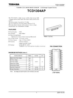
2 The USB4000 operates from the +5V power, provided through the USB, or from a separate power supply and an RS-232 interface. 211-00000-000-05-201604 1. USB4000 data Sheet The detector used in the USB4000 spectrometer is a high-sensitivity 3648-element CCD array from Toshiba, product number TCD1304AP. (For complete details on this detector, visit Toshiba's web site at Ocean Optics applies a coating to all TCD1304AP detectors, so the optical sensitivity could vary from that specified in the Toshiba datasheet). The USB4000 operates off of a single +5 VDC supply and either a USB or RS-232 interface. It has a 22-pin external interface to easily integrate with Ocean Optics ' other modular components for an entire system. A special 500 lines/mm groove density grating option used in the USB4000 XR spectrometer provides broader spectral coverage with no sacrifice in performance. This extended-range spectrometer is preconfigured with this new grating for general-purpose UV-NIR applications.
3 Features TCD1304AP Detector High-sensitivity detector Readout rate: 1 MHz Shutter mode Responsive from 200 to 1100 nm, specific range and resolution depends on your grating and entrance slit choices Sensitivity of up to 130 photons/count at 400 nm; 60 photons/count at 600 nm An optical resolution of (FWHM). A wide variety of Optics available 14 gratings, plus Grating #31for the XR version 6 slit widths 3 detector coatings 6 optical filters Integration times from ms to 10 seconds 16-bit, 3 MHz A/D Converter Embedded microcontroller allows programmatic control of all operating parameters and standalone operation USB 480 Mbps (high speed) and 12 Mbps (full speed). RS232 115K baud Multiple communication standards for digital accessories (SPI, I2C). Onboard Pulse Generator 2 programmable strobe signals for triggering other devices Software control of nearly all pulse parameters Onboard GPIO 8 user-programmable digital I/O. EEPROM storage for Wavelength Calibration Coefficients Linearity Correction Coefficients Absolute Irradiance Calibration (optional).
4 Low power consumption of only 250 mA @ 5 VDC. 2 211-00000-000-05-201604. USB4000 data Sheet 5 triggering modes 24-pin connector for interfacing to external products Programmable for standalone operation CE Certification Specifications Specifications Criteria Absolute Maximum Ratings: VCC + VDC. Voltage on any pin Vcc Physical Specifications: Physical Dimensions mm x mm x mm Weight 190 g Power: Power requirement (master) 230 mA at +5 VDC. Supply voltage V. Power-up time ~5s depending on code size Spectrometer: Design Asymmetric crossed Czerny-Turner Focal length (input) 42mm Focal length (output) 68mm (75, 83, and 90mm focal lengths are also available). Input Fiber Connector SMA 905. Gratings 14 different gratings, , plus Grating #31 for the XR version Entrance Slit 5, 10, 25, 50, 100, or 200 m slits. (Slits are optional. In the absence of a slit, the fiber acts as the entrance slit.). Detector Toshiba TCD1304AP linear CCD array nd rd Filters 2 and 3 order rejection, long pass (optional).
5 Spectroscopic: Integration Time ms 10 seconds 8. Dynamic Range 2 x 10 (system); 1000:1 for a single acquisition Signal-to-Noise 300:1 (at full signal). Dark Noise 24 counts RMS for 32000 count saturation 50 counts RMS for 65000 count saturation Resolution (FWHM) nm FWHM (varies by configuration). Spectrometer Channels One Environmental Conditions: Temperature -30 to +70 C Storage & -10 to +50 C Operation Humidity 0% - 90% noncondensing Interfaces: USB USB , 480 Mbps RS-232 2-wire RS-232. 211-00000-000-05-201604 3. USB4000 data Sheet Mechanical Diagram Figure 1: USB4000 Outer Dimensions 4 211-00000-000-05-201604. USB4000 data Sheet Electrical Pinout Listed below is the pin description for the USB4000 Accessory Connector located on the front vertical wall of the unit. The connector is a Samtec part # IPT1-111-01-S-D-RA connector. The vertical mate to this is part #IPS1-111-01-S-D-VS and the right angle PCB mount is part #IPS1-111-01-S-D-RA. Pin Function Input/Output Description #.
6 Input power pin for USB4000 When operating via USB, this VCC, VUSB, or Input or 1 pin can power other peripherals Ensure that peripherals 5 VIN Output comply with USB specifications RS232 transmit signal Communicates with a computer over 2 RS232 Tx Output DB9 Pin 2. RS232 receive signal Communicates with a computer over 3 RS232 Rx Input DB9 Pin 3. TTL signal driven Active HIGH when the Lamp Enable 4 Lamp Enable Output command is sent to the spectrometer Continuous TTL output signal used to pulse a strobe Divided down from 5 Output Strobe the master clock signal 6 Ground Input/Output Ground External TTL input trigger signal See External Triggering Options 7 Input Trigger In document for info TTL output pulse used as a strobe signal Has a programmable 8 Single Strobe Output delay relative to the beginning of the spectrometer integration period 2 2. 2 The I C clock signal for communications to other I C. 9 I C SCL Input/Output peripherals. 2 2 2. 10 I C SDA Input/Output The I C data signal for communications to other I C peripherals.
7 SPI Master Out Slave In (MOSI) signal for communication to 11 MOSI Output other SPI peripherals SPI Master In Slave Out (MISO) signal for communication to 12 MISO Input other SPI peripherals 13 GPIO-1(1P)* Input/Output Master clock 211-00000-000-05-201604 5. USB4000 data Sheet Pin Function Input/Output Description #. 14 GPIO-0(2P)* Input/Output Base clock 15 GPIO-3(1N)* Input/Output Integration clock 16 GPIO-2(2N)* Input/Output Reserved 17 GPIO-5(3P)* Input/Output Acquire Spectra (Read Enable). 18 GPIO-4(4P)* Input/Output Reserved 19 GPIO-7(3N)* Input/Output Reserved 20 GPIO-6(4N)* Input/Output Reserved A1 SPI_CLK Output SPI clock signal for communication to other SPI peripherals The SPI Chip/Device Select signal for communications to other A2 SPICS OUT Output SPI peripherals NOTE: GPIO nP and nN are for future LVDS capability CCD Overview CCD Detector The detector used for the USB4000 is a charge transfer device (CCD) that has a fixed well depth (capacitor) associated with each photodetector (pixel).
8 Charge transfer, reset and readout initiation begin with the integration time clock going HIGH. At this point, the remaining charge in the detector wells is transferred to a shift register for serial transfer. This process is how the array is read. The reset function recharges the photodetector wells to their full potential and allows for nearly continuous integration of the light energy during the integration time, while the data is read out through serial shift registers. At the end of an integration period, the process is repeated. When a well is fully depleted by leakage through the back-biased photodetector, the detector is considered saturated and provides the maximum output level. The CCD is a depletion device and thus the output signal is inversely proportional to the input photons. The electronics in the USB4000 invert and amplify this electrical signal. 6 211-00000-000-05-201604. USB4000 data Sheet CCD Detector Reset Operation At the start of each integration period, the detector transfers the signal from each pixel to the readout registers and resets the pixels.
9 The total amount of time required to perform this operation is ~12 s. The user needs to account for this time delay when the pixels are optically inactive, especially in the external triggering modes. Signal Averaging Signal averaging is an important tool in the measurement of spectral structures. It increases the S:N. and the amplitude resolution of a set of samples. The types of signal averaging available in our software are time-based and spatial-based. When using the time-base type of signal averaging, the S:N increases by the square root of the number of samples. Signal averaging by summing is used when spectra are fairly stable over the sample period. Thus, a S:N of 3000:1 is readily achieved by averaging 100 spectra. Spatial averaging or pixel boxcar averaging can be used to improve S:N when observed spectral structures are broad. The traditional boxcar algorithm averages n pixel values on each side of a given pixel. Time-based and spatial-based algorithms are not correlated, so therefore the improvement in S:N is the product of the two processes.
10 In review, large-well devices are far less sensitive than small-well devices and thus, require a longer integration time for the same output. Large-well devices achieve a good S:N because they integrate out photon noise. Small-well devices must use mathematical signal averaging to achieve the same results as large-well devices, but small-well devices can achieve the results in the same period of time. This kind of signal averaging was not possible in the past because analog-to-digital converters and computers were too slow. Large-well devices consume large amounts of power, resulting in the need to build thermoelectric coolers to control temperature and reduce electronic noise. Then, even more power is required for the temperature stabilization hardware. But, small-well devices only need to use signal averaging to achieve the same results as large-well devices, and have the advantages of remaining cool and less noisy. Internal Operation Pixel Definition A series of pixels in the beginning of the scan have been covered with an opaque material to compensate for thermal induced drift of the baseline signal.