Transcription of VIN AP2127 300mA HIGH SPEED, EXTREMELY LOW NOISE …
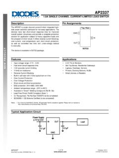
1 AP2127 Document number: DS36478 Rev. 7 - 2 1 of 24 December 2017 Diodes Incorporated AP2127 300mA high speed , EXTREMELY LOW NOISE cmos LDO REGULATOR Description The AP2127 Series are positive voltage regulator ICs fabricated by cmos process. The AP2127 Series have features of low dropout voltage, low NOISE , high output voltage accuracy, and low current consumption which make them ideal for use in various battery-powered devices. The AP2127 has , , , , , , , , , and fixed voltage versions and to adjustable voltage versions. The AP2127 Series are available in SOT-23 (for fixed versions only), SOT-23-3 (for fixed versions only), SOT-23-5, SOT-89 (for fixed versions only) packages.
2 Features Wide Operating Voltage: to 6V high Output Voltage Accuracy: 2% high Ripple Rejection: 68dB @ f = 1kHz, 54dB @ f = 10kHz Low Standby Current: A Low Dropout Voltage: 170mV @ 300mA for VOUT = , 140mV @ 300mA for VOUT = Low Quiescent Current: 60 A Typical Low Output NOISE : 60 VRMS @VOUT = Short Current Limit: 50mA Over Temperature Protection Compatible with Low ESR Ceramic Capacitor: 1 F for CIN and COUT Excellent Line/Load Regulation Soft Start Time: 50 s Auto Discharge Resistance: RDS(ON) = 60 Totally Lead-Free & Fully RoHS Compliant (Notes 1 & 2) Halogen and Antimony Free. Green Device (Note 3) Pin Assignments (Top View) (Top View) SOT-23/SOT-23-3 SOT-23-5 (Top View) SOT-89 Applications Datacom Notebook Computers Mother Board Notes: 1.
3 No purposely added lead. Fully EU Directive 2002/95/EC (RoHS) & 2011/65/EU (RoHS 2) compliant. 2. See for more information about Diodes Incorporated s definitions of Halogen- and Antimony-free, "Green" and Lead-free. 3. Halogen- and Antimony-free "Green products are defined as those which contain <900ppm bromine, <900ppm chlorine (<1500ppm total Br + Cl) and <1000ppm antimony compounds. 321 VINVOUTGND12345 VINGNDVOUTS hutdownNC/ADJ123 GNDVINVOUT AP2127 Document number: DS36478 Rev. 7 - 2 2 of 24 December 2017 Diodes Incorporated AP2127 Typical Applications Circuit VINVINVOUTVOUTADJS hutdownGNDCOUT1 FCIN1 FR1R2AP212713245 VOUT = (1+R1/R2)V VINVINVOUTVOUTS hutdownGNDCOUT1 FCIN1 FAP21271325 For Fixed Voltage Versions AP2127 Document number: DS36478 Rev.
4 7 - 2 3 of 24 December 2017 Diodes Incorporated AP2127 Pin Descriptions Pin Name Pin Number Function SOT-23 SOT-23-3 SOT-23-5 SOT-89 VIN 3 1 2 Power Input VOUT 2 5 3 Power Output GND 1 2 1 Ground NC/ADJ 4 No Connection / VOUT feedback input, connect resistor divider. Shutdown 3 Enable Input. PAD Exposed PAD for thermal performance improvement connect to GND Functional Block Diagram ShutdownGNDVINVOUTS hutdown AndLogic ControlCurrent LimitAndThermalProtectionMOS DriverVREF1523 Fixed Version (SOT-23-5 Package) Shutdown And Logic ControlCurrent LimitAndThermalProtectionMOS DriverVREFS hutdownGNDVINVOUTADJ15234 Adjustable Version (SOT-23-5 Package) AP2127 Document number: DS36478 Rev. 7 - 2 4 of 24 December 2017 Diodes Incorporated AP2127 Absolute Maximum Ratings (Note 4) (@TA = +25 C, unless otherwise specified.)
5 Symbol Parameter Value Unit VIN Input Voltage V VCE Shutdown Input Voltage to VIN + V IOUT Output Current 450 mA TJ Junction Temperature +150 C TSTG Storage Temperature Range -65 to +150 C TLEAD Lead Temperature (Soldering, 10sec) +260 C JA Thermal Resistance (Junction to Ambient) SOT-23 180 C/W SOT-23-3 250 SOT-23-5 250 SOT-89 100 ESD ESD (Human Body Model) 6000 V ESD ESD (Machine Model) 200 V Note: 4. Stresses greater than those listed under "Absolute Maximum Ratings" may cause permanent damage to the device. These are stress ratings only, and functional operation of the device at these or any other conditions beyond those indicated under "Recommended Operating Conditions" is not implied. Exposure to "Absolute Maximum Ratings" for extended periods may affect device reliability.
6 Recommended Operating Conditions (@TA = +25 C, unless otherwise specified.) Symbol Parameter Min Max Unit VIN Input Voltage 6 V TA Operating Ambient Temperature Range -40 +85 C AP2127 Document number: DS36478 Rev. 7 - 2 5 of 24 December 2017 Diodes Incorporated AP2127 Electrical Characteristics (VIN = (for to voltage versions), VIN = VOUT +1V (for to voltage versions), VIN = 6V @ VOUT = , TA = +25 C, CIN = 1 F, COUT = 1 F, Bold typeface applies over -40 C TA +85 C, unless otherwise specified.) Symbol Parameter Conditions Min Typ Max Unit VREF Reference Voltage VIN = VOUT +1V 1mA IOUT 300mA V VOUT Output Voltage VIN = VOUT +1V 1mA IOUT 300mA 98% x VOUT 102% x VOUT V VIN Input Voltage 6 V IOUT(MAX)
7 Maximum Output Current VIN - VOUT = 1V VOUT = x VOUT 300 400 mA VOUT Load Regulation VIN - VOUT = 1V 1mA IOUT 300mA 4 10 mV VOUT Line Regulation VOUT + VIN 6V IOUT = 30mA 5 mV VDROP Dropout Voltage VOUT = , IOUT = 300mA 1400 1500 mV VOUT = , IOUT = 300mA 1200 1300 VOUT = , IOUT = 300mA 900 1000 VOUT = , IOUT = 300mA 600 700 VOUT = , , , , , IOUT = 300mA 170 300 VOUT = , IOUT = 300mA 140 300 IQ Quiescent Current VIN = VOUT +1V, IOUT = 0mA 60 90 A ISTD Standby Current VIN = VOUT +1V VSHUTDOWN in off mode A PSRR Power Supply Rejection Ration to , Ripple 1VP-P VIN = VOUT +1V f = 100Hz 68 dB f = 1kHz 68 dB f = 10kHz 54 dB , Ripple VIN = VOUT +1V f = 100Hz 63 dB f = 1kHz 63 dB f = 10kHz 45 dB VOUT/VOUT / T Output Voltage Temperature Coefficient IOUT = 30mA, -40 C TA +85 C 100 ppm/ C ISHORT Short Current Limit VOUT = 0V 50 mA tSS Soft Start Time 50 s VNOISE RMS Output NOISE TA = +25 C, 10Hz f 100kHz, VOUT = 60 VRMS Shutdown high Voltage Shutdown Input Voltage high V Shutdown Low Voltage Shutdown Input Voltage Low V VOUT Discharge MOSFET RDS(ON)
8 Shutdown Input Voltage Low 60 Shutdown Pull Down Resistance 3 M Thermal Shutdown +165 C Thermal Shutdown Hysteresis +30 JC Thermal Resistance SOT-23 100 C/W SOT-23-3 150 SOT-23-5 150 SOT-89 75 AP2127 Document number: DS36478 Rev. 7 - 2 6 of 24 December 2017 Diodes Incorporated AP2127 Performance Characteristics (Note 5) Output Voltage vs. Case Temperature Output Voltage vs. Case Temperature Output Voltage vs. Case Temperature Output Voltage vs. Input Voltage Output Voltage vs.
9 Input Voltage Output Voltage vs. Input Voltage Note 5: Maximum output of passed qualification test. Performance Characteristics for are for reference only. Output Voltage (V)Case Temperature (oC) IOUT=10mA IOUT=150mA IOUT=300mAVIN= Output Voltage (V)Case Temperature (oC) IOUT=10mA IOUT=150mA IOUT=300mAVIN= Output Voltage (V)Case Temperature (oC) IOUT=10mA IOUT=150mA IOUT=300mAVIN=6V, VOUT= Output Voltage (V)Input Voltage (V) IOUT=0 IOUT=300mATC=25oCVOUT= Output Voltage (V)Input Voltage (V) IOUT=0 IOUT=300mATC=25oC, VOUT= Output Voltage (V)Input Voltage (V) IOUT=0 IOUT=300mATC=25oC, VOUT= AP2127 Document number: DS36478 Rev.
10 7 - 2 7 of 24 December 2017 Diodes Incorporated AP2127 Performance Characteristics (Cont.) (Note 5) Output Voltage vs. Output Current Output Voltage vs. Output Current Output Voltage vs. Output Current Output Voltage vs. Output Current Quiescent Current vs. Input Voltage Quiescent Current vs. Input Voltage Note 5: Maximum output of passed qualification test. Performance Characteristics for are for reference only. Output Voltage (V)Output Current (A) TC=-40oC TC=25oC TC=85oCVIN= Output Voltage (V)Output Current (A) TC=-40oC TC=25oC TC=85oCVIN= , VOUT= Output Voltage (V)Output Current (A) VIN= VIN= VIN=6 VTC=25oC, VOUT= Output Voltage (V)Output Current (A) TC=-40oC TC=25oC TC=85oCVIN=6V, VOUT= Quiescent Current ( A)Input Voltage (V) TC=-40oC TC=25oC TC=85oCIOUT=0 VOUT= Quiescent Current ( A)Input Voltage (V) TC=-40oC TC=25oC TC=85oCIOUT=0, VOUT= AP2127 Document number: DS36478 Rev.
