Transcription of Voltage comparators
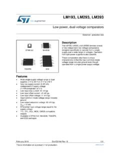
1 September 2006 Rev 41/1414LM111-LM211-LM311 Voltage comparator with strobeFeatures Maximum input current: 150nA Maximum offset current: 20nA Differential input Voltage range: 30V Power consumption:135mW at 15V Supply Voltage : +5V to 15V Output current: 50mADescriptionThe LM111, LM211, LM311 are Voltage comparators that have low input are also designed to operate over a wide range of supply voltages: from standard 15V operational amplifier supplies down to the single +5V supply used for IC output is compatible with RTL-DTL and TTL as well as MOS circuits and can switch voltages up to +50V at output currents as high as codesDSO-8(Plastic micropackage)NDIP8(Plastic package)Pin connections (top view)Part numberTemperature rangePackagePackingMarkingLM211N-40 C, +105 CDIP8 TubeLM211 NLM211D/DTSO-8 Tube or tape & reel211LM311N0 C, +70 CDIP8 TubeLM311LM311D/DTSO-8 Tube or Tape & Contents1 Schematic diagram.
2 32 Absolute maximum ratings & operating conditions .. 43 Electrical characteristics .. 54 Typical application schematics .. 95 Package mechanical data .. package .. package .. 126 Revision history .. 13LM111-LM211-LM311 Schematic diagram 3/141 Schematic diagramFigure diagramAbsolute maximum ratings & operating conditionsLM111-LM211-LM3114/14 2 Absolute maximum ratings & operating conditions Table maximum ratings (AMR)SymbolParameterValueUnitVCCS upply Voltage 36 VVidDifferential input Voltage 30 VViInput Voltage (1)1. This rating applies for 15V supplies. The positive input Voltage limit is 30V above the negative.
3 The negative input Voltage is equal to the negative supply Voltage or 30V below the positive supply, whichever is less. 15VV(1-4)Ground to negative supply voltage30VV(7-4)Output to negative supply voltageLM111-LM211LM3115040 VOutput short-circuit duration10sVoltage at strobe pinVCC+ -5 VpdPower dissipation (2)DIP8SO-82. Pd is calculated with Tamb = +25 C, Tj = +150 C and Rthja = 100 C/W for the DIP8 package, and Rthja= 175 C/W for the SO-8 temperature+150 CTstgStorage temperature range-65 to +150 CTable conditionsSymbolParameterValueUnitVCCS upply voltage5 to 15 VToperOperating free-air temperature rangeLM111LM211LM311-55 to +125-40 to +1050 to +70 CLM111-LM211-LM311 Electrical characteristics 5/143 Electrical characteristics Table + = 15V, Tamb = +25 C (unless otherwise specified)SymbolParameterConditionsLM111 - Max.
4 Offset Voltage (1)RS 50k Tamb = +25 CTmin Tamb offset current (1)Tamb = +25 CTmin Tamb Tmax4102065070nAIibInput bias current (1)Tamb = +25 CTmin Tamb Tmax60100150100250300nAAvdLarge signal Voltage gain4020040200V/mVICC+ICC-Supply currents common mode Voltage rangeTmin Tamb + +13 + +13 VVOLLow level output voltageTamb = +25 C, IO = 50mA, Vi = +25 C, IO = 50mA, Vi Tamb TmaxVCC+ + , VCC- = 0IO = 8mA, Vi Tamb TmaxVCC+ + , VCC- = 0IO = 8mA, Vi level output currentTamb = +25 CVi +5mV, VO = + = +25 CVi +10mV, VO = + Tamb TmaxVi +5mV, VO = + AIstrobeStrobe current33mAtreResponse time (2)200200ns1. The offset Voltage , offset current and bias current specifications apply for any supply Voltage from a single +5V supply up to 15V supplies.
5 The offset voltages and offset currents given are the maximum values required to drive the output down to +1V or up to +14V with a 1mA load current. Thus, these parameters define an error band and take into account the worst-case of Voltage gain and input The response time specified is for a 100mV input step with 5mV overdrive. Electrical characteristicsLM111-LM211-LM3116/14 LM111-LM211-LM311 Electrical characteristics 7/14 Electrical characteristicsLM111-LM211-LM3118/14 LM111-LM211-LM311 Typical application schematics 9/144 Typical application schematics Package mechanical dataLM111-LM211-LM31110/14 5 Package mechanical dataIn order to meet environmental requirements, STMicroelectronics offers these devices in ECOPACK packages.
6 These packages have a Lead-free second level interconnect. The category of second level interconnect is marked on the package and on the inner box label, in compliance with JEDEC Standard JESD97. The maximum ratings related to soldering conditions are also marked on the inner box label. ECOPACK is an STMicroelectronics trademark. ECOPACK specifications are available at: mechanical data 11 DIP8 package DIP-8 MECHANICAL DATAP001 FPackage mechanical dataLM111-LM211-LM31112/14 SO-8 package (max.) MECHANICAL DATA0016023/C 8LM111-LM211-LM311 Revision history 13/146 Revision history DateRevisionChanges1-Jun-021 Initial 3.
7 On page 5 changes connections updated on page description under title on cover Please Read Carefully:Information in this document is provided solely in connection with ST products. STMicroelectronics NV and its subsidiaries ( ST ) reserve theright to make changes, corrections, modifications or improvements, to this document, and the products and services described herein at anytime, without ST products are sold pursuant to ST s terms and conditions of are solely responsible for the choice, selection and use of the ST products and services described herein, and ST assumes noliability whatsoever relating to the choice, selection or use of the ST products and services described license, express or implied, by estoppel or otherwise, to any intellectual property rights is granted under this document.
8 If any part of thisdocument refers to any third party products or services it shall not be deemed a license grant by ST for the use of such third party productsor services, or any intellectual property contained therein or considered as a warranty covering the use in any manner whatsoever of suchthird party products or services or any intellectual property contained OTHERWISE SET FORTH IN ST S TERMS AND CONDITIONS OF SALE ST DISCLAIMS ANY EXPRESS OR IMPLIEDWARRANTY WITH RESPECT TO THE USE AND/OR SALE OF ST PRODUCTS INCLUDING WITHOUT LIMITATION IMPLIEDWARRANTIES OF MERCHANTABILITY, FITNESS FOR A PARTICULAR PURPOSE (AND THEIR EQUIVALENTS UNDER THE LAWSOF ANY JURISDICTION), OR INFRINGEMENT OF ANY PATENT, COPYRIGHT OR OTHER INTELLECTUAL PROPERTY EXPRESSLY APPROVED IN WRITING BY AN AUTHORIZED ST REPRESENTATIVE, ST PRODUCTS ARE NOTRECOMMENDED, AUTHORIZED OR WARRANTED FOR USE IN MILITARY, AIR CRAFT, SPACE, LIFE SAVING, OR LIFE SUSTAININGAPPLICATIONS, NOR IN PRODUCTS OR SYSTEMS WHERE FAILURE OR MALFUNCTION MAY RESULT IN PERSONAL INJURY,DEATH, OR SEVERE PROPERTY OR ENVIRONMENTAL DAMAGE.
9 ST PRODUCTS WHICH ARE NOT SPECIFIED AS "AUTOMOTIVEGRADE" MAY ONLY BE USED IN AUTOMOTIVE APPLICATIONS AT USER S OWN of ST products with provisions different from the statements and/or technical features set forth in this document shall immediately voidany warranty granted by ST for the ST product or service described herein and shall not create or extend in any manner whatsoever, anyliability of and the ST logo are trademarks or registered trademarks of ST in various in this document supersedes and replaces all information previously ST logo is a registered trademark of STMicroelectronics. All other names are the property of their respective owners. 2006 STMicroelectronics - All rights reservedSTMicroelectronics group of companiesAustralia - Belgium - Brazil - Canada - China - Czech Republic - Finland - France - Germany - Hong Kong - India - Israel - Italy - Japan - Malaysia - Malta - Morocco - Singapore - Spain - Sweden - Switzerland - United Kingdom - United States of