Transcription of ZXBM5210 Description Pin Assignments - Diodes …
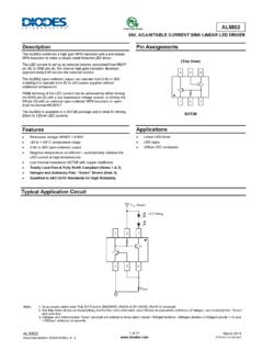
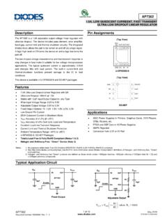
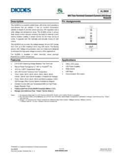
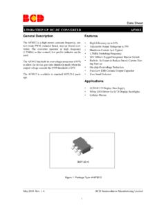
1 ZXBM5210 Document number: DS36765 Rev. 1 - 2 1 of 17 December 2013 Diodes incorporated NEW PRODUCT ZXBM5210 REVERSIBLE DC MOTOR DRIVE WITH SPEED CONTROL Description The ZXBM5210 is a single chip solution for driving a single-coil reversible direct current (DC) fans and motors. The integrated full-bridge driver output stage is designed to minimize audible switching noise and electromagnetic interference (EMI) providing a low noise solution For system flexibility, the device has four modes of operation: Forward, Reverse, Brake and Standby selected via FWD and REV pins.
2 The Forward and Reverse modes provide the motor rotation direction control, the Brake mode allows quick stop and the Standby mode helps system efficiency by powering down most of the internal circuits to consume less than 32uA typical. The motor speed can be adjusted by changing the duty ratio of the PWM signal on the FWD or REV pins in the PWM mode or alternatively by adjusting DC voltage input signal to the VREF pin in the VREF speed control mode. To help protect the IC and the motor coil the ZXBM5210 includes under voltage, over voltage, over current and over temperature protections.
3 Once the safe operating range has been exceeded the device shuts down the output drive to help prevent over stress on the IC or the coil. The device internal current protection threshold is typical. The ZXBM5210 is available in the standard SO8 and thermally enhanced SO8-EP packages. Features Supports single-coil reversible DC motor applications Operating voltage: 3V to 18V Four modes of operations: Forward, Reverse, Brake and Standby Low quiescent current of typical in normal operation and 32 A in standby mode Internal over current protection Under voltage lockout and over voltage protection Over temperature protection -40 C to +85 C /105 C operating temperature 6kV ESD withstand capability Standard SO-8 and thermally enhanced SO-8EP Totally Lead-Free & Fully RoHS Compliant (Notes 1 & 2) Halogen and Antimony Free.
4 Green Device (Note 3) Pin Assignments SO-8 SO-8EP Applications 5V / 9V/ 12V / 15V DC reversible motors and actuators Home appliances Handheld power tools Valve open and close Remote control motorized toys Medium Voltage/ Low Power DC Motors Notes: 1. No purposely added lead. Fully EU Directive 2002/95/EC (RoHS) & 2011/65/EU (RoHS 2) compliant. 2. See for more information about Diodes incorporated s definitions of Halogen- and Antimony-free, "Green" and Lead-free. 3. Halogen- and Antimony-free "Green products are defined as those which contain <900ppm bromine, <900ppm chlorine (<1500ppm total Br + Cl) and <1000ppm antimony compounds.
5 ZXBM5210 Document number: DS36765 Rev. 1 - 2 2 of 17 December 2013 Diodes incorporated NEW PRODUCT ZXBM5210 Typical Applications Circuit Note: 4. C1 is for power stabilization and to strengthen the noise immunity, the recommended capacitance is 100nF to 1 F or more. C2 is a re-circulating capacitor for back rush voltage and recommended capacitance is 100nF for low current applications to 10 F or more for large current applications. See application note section Pin descriptions Package: SO-8 Pin # Pin Name Function 1 OUT1 Driver output 2 VM Power Supply Voltage 3 VDD Power Supply Voltage 4 FWD Forward Control Input (logic level, max) 5 REV Reverse Control Input (logic level, max) 6 VREF Input reference voltage to set the internal PWM oscillator duty ratio 7 OUT2 Driver Output 8 GND Ground Package.
6 SO8-EP Pin # Pin Name Function 1 OUT1 Driver output 2 VM Power Supply Voltage 3 VDD Power Supply Voltage 4 FWD Forward Control Input (logic level, max) 5 REV Reverse Control Input (logic level, max) 6 VREF Input reference voltage to set the internal PWM oscillator duty ratio 7 OUT2 Driver Output 8 GND Ground Pad Pad The exposed pad is for thermal dissipation and it is internally connected to the ground.
7 On the PCB layout, it can be connected to GND or left open circuit. ZXBM5210 Document number: DS36765 Rev. 1 - 2 3 of 17 December 2013 Diodes incorporated NEW PRODUCT ZXBM5210 Functional Block Diagram Absolute Maximum Ratings (Note 5) @TA = +25 C, unless otherwise specified.) Symbol Characteristic Values Unit VM and VDD, Supply voltage (Note 6) 24 V VOUT1, VOUT2 VREF All other pins except FWD and REV pins 24 V VFWD and VREV FWD and REV pin voltage 7 V VREVERSE Reverse supply Voltage on all pins V IOUTPUT Output current (source and sink)
8 - Peak 1500 mA PD Package power dissipation SO8 (Note 7) 1043 mW SO8-EP (Note 8) 2980 mW Ts Storage temperature range -65 to +150 C TJ Maximum junction temperature 150 C ESD HBM Human Body Model ESD withstand capability VDD, VM, VREF, FWD, REV, GND and OUT1 OUT2 pins 6 kV Notes: 5. Stresses greater than the 'Absolute Maximum Ratings' specified above, may cause permanent damage to the device. These are stress ratings only; functional operation of the device at these or any other conditions exceeding those indicated in this specification is not implied.
9 Device reliability may be affected by exposure to absolute maximum rating conditions for extended periods of time 6. The absolute maximum supply voltage of 24V is a transient stress rating and is not meant as a functional operating condition. It is not recommended to operate the device at the absolute maximum rated conditions for any period of time. 7. SO-8 soldered to minimum recommended landing pads (see Package Outline Dimension section) on a 1 x1 two-layer FR4 PCB ( thickness) without any via or copper flood on the bottom layer.
10 See thermal de-rating curves in the thermal performance section. 8. SO-8EP exposed pad soldered to minimum recommended landing pads (see Package Outline Dimension section) on a 2 x2 two-layer FR4 PCB ( thickness) with four thermal vias in the exposed PAD to the copper flood on the bottom layer. See thermal de-rating curves in the thermal performance section. Recommended Operating Conditions Symbol Characteristic Conditions Min Max Unit VDD Supply Voltage Operating 3 18 V TA Operating Temperature Range Operating, SO8 package -40 +85 C Operating, SO8-EP package -40 +105 C ZXBM5210 Document number: DS36765 Rev.
