Cmos Logic
Found 10 free book(s)
DESIGNING COMBINATIONAL LOGIC GATES IN CMOS
bwrcs.eecs.berkeley.eduLOGIC GATES IN CMOS In-depth discussion of logic families in CMOS—static and dynamic, pass-transistor, nonra-n tioed and ratioed logic n Optimizing a logic gate for area, speed, energy, or robustness Low-power and high-performance circuit-design techniques 6.1 Introduction 6.2 Static CMOS Design 6.2.1 Complementary CMOS 6.5 Leakage in Low ...
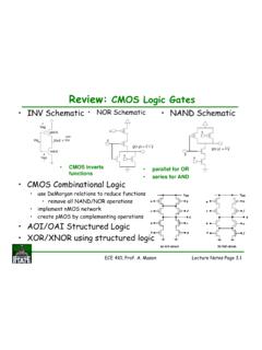
Review: CMOS Logic Gates - Michigan State University
www.egr.msu.eduReview: CMOS Logic Gates • NOR Schematic x x y g(x,y) = x y x x y g(x,y) = x + y cit•NmaeNA SDhc • parallel for OR • series for AND • INV Schematic + Vgs-Vin Vout pMOS nMOS + Vsg-= Vin • CMOS inverts functions • CMOS Combinational Logic • use DeMorgan relations to reduce functions • remove all NAND/NOR operations • implement ...
AD9851 CMOS 180 MHz DDS/DAC Synthesizer Data Sheet …
www.analog.comCMOS LOGIC INPUTS Logic 1 Voltage, 5 V Supply 25°C I 3.5 V Logic 1 Voltage, 3.3 V Supply 25°C IV 2.4 V Logic 1 Voltage, 2.7 V Supply 25°C IV 2.0 V ...

10.3 CMOS Logic Gate Circuits - ITTC
www.ittc.ku.edu11/14/2004 Example Another CMOS Logic Gate Synthesis.doc 2/4 Jim Stiles The Univ. of Kansas Dept. of EECS And thus: YABC= + ′ Therefore, the inputs to this logic gate should be A, B, and C’ (i.e, A, B, and the complement of C ). Note that this Boolean expression “says” that: “The ouput is low if either,A AND B are both high, OR C ...
CMOS image sensor fabrication technologies Pixel design ...
isl.stanford.eduStandard CMOS logic transistors to reduce power consumption and attain high circuit speed Similar strategy as DRAM Separate \array" transistors, and \support circuit" transistors EE 392B: Device and Fabrication 5-25. Pixel Layout and Pixel Size Pixel size mostly determined by …

Jessica Clements English 626: Postmodernism, Rhetoric ...
owl.purdue.eduNov 07, 2019 · inner logic. ”3 Science, so the ... 17th edition of CMOS (section 14.34). 3 which accounted for the “unbridled individualism of great thinkers, the great benefactors of humankind, who through their singular efforts and struggles would push reason and civilization willy-nilly to the point of true emancipation. ...
ICM7555 General purpose CMOS timer - NXP
www.nxp.comGeneral purpose CMOS timer 8. Limiting values [1] Due to the SCR structure inherent in the CMOS process used to fabricate these devices, connecting any terminal to a voltage greater than VDD + 0.3 V or less than GND −0.3 V may cause destructive latch-up. For this reason it is recommended that no inputs from
PCF8563 Real-time clock/calendar - NXP
www.nxp.com1 all RTC divider chain flip-flops are asynchronously set to logic 0; the RTC clock is stopped (CLKOUT at 32.768 kHz is still available) 4N 0[2] unused 3 TESTC 0 Power-On Reset (POR) override facility is disabled; set to logic 0 for normal operation Section 8.11.1 1[1] Power-On Reset (POR) override may be enabled 2to0 N 000[2] unused

Data Sheet ADP1763 - Analog Devices
www.analog.comFeb 03, 2022 · Logic Input High EN. HIGH. 595 625 690 mV Low EN. LOW. 550 580 630 mV Input Logic Hysteresis EN. HYS. 45 mV Input Leakage Current I. EN-LKG. EN = V. IN. or GND 0.01 1 µA Input Delay Time tI. EN-DLY. From EN rising from 0 V to V. IN. to 0.1 × V. OUT. 100 µs UNDERVOLTAGE LOCKOUT UVLO Input Voltage Rising UVLO. RISE. T. J = −40°C to …

Omni ision Preliminary Datasheet Advanced Information
web.mit.eduOV7670/OV7171 CMOS VGA (640x480) CAMERACHIPTM Sensor Omni ision ® with OmniPixel® Technology General Description The OV7670/OV7171 CAMERACHIPTM image sensor is a low voltage CMOS device that provides the full functionality of a single-chip VGA camera and image processor in a small footprint package.