
CMOS Capacitance and Circuit Delay
Capacitance CSD has a bottom and out-side perimeter between the source or drain and the underlying substrate which is connected to a.c. ground. There is also a gate perimeter component for which there is a 2X magnifying (Miller) effect on the S/D side because the
Download CMOS Capacitance and Circuit Delay

Information
Domain:
Source:
Link to this page:
Documents from same domain
Diodes and Transistors
inst.eecs.berkeley.eduDiodes and Transistors 1. ... basic semiconductor physics. We won’t discuss the details because the point of this ... switch. Below the specified ...
HSPICE Tutorial - University of California, Berkeley
inst.eecs.berkeley.eduHSPICE Tutorial Contents 1 Introduction 1 ... ee105 spice tutorial example 1 - simple rc circuit in the Results Browser and double-clicking vs and vo to plot them in the graph. You may have been able to guess from the netlist, but you’ll see that vsis a …
Introduction to LabVIEW - University of California, …
inst.eecs.berkeley.eduIntroduction to LabVIEW 1. Introduction Welcome to the LabVIEW component of EE100! This lab is just a simple introduction to the graphical circuit simulation ...
Introduction to LabVIEW For Use in Embedded …
inst.eecs.berkeley.eduUC Berkeley EE249 Hugo.Andrade@ni.com Introduction to LabVIEW For Use in Embedded System Development
EE105 –Fall 2015 Microelectronic Devices and Circuits
inst.eecs.berkeley.eduSummary of MOS Single-Transistor Amplifiers MOS Common Source Common Source with Deg. Common Drain Common Gate Ri ∞ ∞ ∞ Small Ro Large Very Large Small Large
Introduction to Digital Systems - University of …
inst.eecs.berkeley.eduDepartment of EECS EE100/42-43 Spring 2007 Rev. 1 Introduction to Digital Systems 0. Acknowledgments Many thanks to Prof. Bernhard Boser and National Instruments for funding this project in the
EE126: Probability and Random Processes - Lecture 1 ...
inst.eecs.berkeley.eduprobability 4 The probabilities summed over all of the base outcomes always equals 1 Example: Toss a fair coin twice 1 Base outcomes are HH,HT,TH,TT 2 This covers all the possibilities. M.E. 3 Each of these outcomes is equally likely 4 Assign each outcome a probability of 0:25. The list (set) of base outcomes is called the Sample Space.
EECS 126 Probability and Random Processes: Course Syllabus ...
inst.eecs.berkeley.eduDescription: Probability is a mathematical discipline that allows one to reason about uncertainty: it helps us to predict uncertain events, to make better decisions under uncertainty, and to design and build systems. Throughout the course, we will teach you the fundamental ideas of probability and random processes along with the labs.
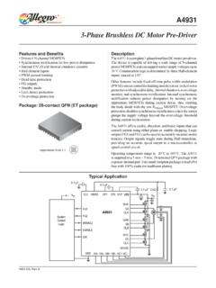
3-Phase Brushless DC Motor Pre-Driver
inst.eecs.berkeley.eduDescription The A4931 is a complete 3-phase brushless DC motor pre-driver . The device is capable of driving a wide range of N-channel power MOSFETs and can support motor supply voltages up to
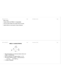
DS -V I G - EECS Instructional Support Group Home Page
inst.eecs.berkeley.eduG D S I D I G-V DS + + V G S _ NMOS I-V CHARACTERISTIC • Since the transistor is a 3-terminal device, there is no single I-V characteristic. • Note that because of the gate insulator, I G = 0 A. • We typically define the MOS I-V characteristic as I D vs. V DS for a fixed V GS. • 3 modes of operation
Related documents

Lecture11-MOS Cap Delay
bwrcs.eecs.berkeley.eduCapacitance [arbitrary units] N+ junction area N+ junction perimeter P+ junction area P+ junction perimeter Junction caps are nonlinear –C J is a function of junction bias EE141 18 EECS141 Lecture #11 18 Linearizing the Junction Capacitance Replace non-linear capacitance by large-signal equivalent linear capacitance
Experiment 8: Capacitance and the Oscilloscope
www.columbia.eduPHYS 1493/1494/2699: Exp. 8 – Capacitance and the oscilloscope 2 Outline Capacitance: − Capacitor as a charge storage device − Capacitors in combination − RC circuits: exponential growth and decay Oscilloscope: − Conversion of analog signals to digital − Display and signal operations Measurements: − Large RC charging − Large RC discharging

2. Features and benefits PRTR5V0U2X - Nexperia
assets.nexperia.comUltra low capacitance double rail-to-rail ESD protection diode 10. Application information Handling data rates up to 480 Mbit/s, USB 2.0 interfaces require ESD protection devices with an extremely low line capacitance in order to avoid signal distortion. With a capacitance of only 1 pF, the device offers IEC 61000-4-2, level 4 compliant ESD ...

ECE 340 Lecture 27 : Junction Capacitance
transport.ece.illinois.eduJunction Capacitance When combine the equations result in the charge on either side of the dipole… Total charge: v Clearly a non-linear function of the applied voltage. Now apply the definition of the capacitance… Junction Capacitance: v •The junction capacitance is a voltage-variable capacitance.

Chapter 5 Capacitance and Dielectrics
web.mit.eduCapacitance and Dielectrics 5.1 Introduction A capacitor is a device which stores electric charge. Capacitors vary in shape and size, but the basic configuration is two conductors carrying equal but opposite charges (Figure

Depletion Capacitance - University of California, Berkeley
inst.eecs.berkeley.eduEE 105 Fall 2000 Page 2 Week 4 Depletion Capacitance (cont.) n break up the charge qJ on the p-side of the junction similarly: total charge in the depletion region = DC charge + small-signal charge qJ = Q J + qj note that the DC charge is a negative number
Chapter 24 – Capacitance and Dielectrics
physics.ucf.edu- Capacitance is a measurement of the ability of capacitor to store energy (V = U / q). Capacitors in Vacuum - Parallel Plate Capacitor: uniform electric field between the plates, charge uniformly distributed over opposite surfaces A Q E εo εo σ = = d A V Q C ab = =ε0 A Qd V E d o ab ε 1 = ⋅ = ε0 = 8.85 x 10⁻¹² F/m

AP Physics Practice Test: Capacitance, Resistance, DC Circuits
www.crashwhite.comCapacitance, Resistance, DC Circuits ©2013, Richard White www.crashwhite.com 4. Three capacitors, of capacitance 1µF, 5µF, and 6µF, are arranged in a circuit with a switch and a 12-V battery as shown above. The equivalent capacitance of the three capacitors is: a. 2 µF b. 3 µF c. 6 µF d. 11/6 µF e. 11/12 µF 5. Two conducting wires, W 1 ...

Chapter Two ELECTROSTATIC POTENTIAL AND …
www.ncert.nic.inand Capacitance 2.3 Figure 2.2 shows some equipotential lines distributed in space. A charged object is moved from point A to point B. (a) The work done in Fig. (i) is the greatest. (b) The work done in Fig. (ii) is least. (c) The work done is the same in Fig. (i), Fig. (ii) and Fig. (iii).