
CMOS Manufacturing Process
Hardened resist Hardened resist Chemical or plasma etch. Digital Integrated Circuits Manufacturing Process EE141 CMOS Process at a Glance Define active areas Etch and fill trenches Implant well regions Deposit and pattern polysilicon layer Implant source and drain regions and substrate contacts
Download CMOS Manufacturing Process

Information
Domain:
Source:
Link to this page:
Documents from same domain
chapter2.fm Page 33 Monday, September 4, 2000 …
bwrcs.eecs.berkeley.eduIC packaging Future Trends in Integrated Circuit Technology 2.1 Introduction 2.2 Manufacturing CMOS Integrated Circuits 2.2.1 The Silicon Wafer 2.2.2 Photolithography 2.2.3 Some Recurring Process Steps ... cess that lies at the core of the semiconductor revolution. Yet, some insight in the steps ...

Designing a Divider - University of California, Berkeley
bwrcs.eecs.berkeley.eduDigital Integrated Circuits 2/e DIVIDE HARDWARE Version 1 ° 64-bit Divisor reg, 64-bit ALU, 64-bit Remainder reg, 32-bit Quotient reg Remainder Quotient Divisor …
Lecture 9: Digital Signal Processors: Applications and ...
bwrcs.eecs.berkeley.eduProcessor Applications General Purpose - high performance ... Digital camera - TMS320C5000 ... DSP evolved from Analog Signal Processors, using analog hardware to transform phyical signals (classical electrical engineering) ASP to DSP because

DESIGNING COMBINATIONAL LOGIC GATES IN CMOS
bwrcs.eecs.berkeley.edu198 DESIGNING COMBINATIONAL LOGIC GATES IN CMOS Chapter 6 6.1Introduction The design considerations for a simple inverter circuit ere presented in the previousw chapter. In this chapter, the design of the inverter will be extended to address the synthesis

DESIGNING SEQUENTIAL LOGIC CIRCUITS
bwrcs.eecs.berkeley.edu272 DESIGNING SEQUENTIAL LOGIC CIRCUITS Chapter 7 7.1 Introduction Combinational logic circuits that were described earlier have the property that the output

Lecture11-MOS Cap Delay
bwrcs.eecs.berkeley.eduEE141 25 EECS141 Lecture #11 25 The Miller Effect V in M1 C gd1 V out ∆V As V in increases, V out drops – Once get into the transition region, gain from V in to V out > 1 So, C gd experiences voltage swing larger than V
Chapter 4 Calculating the Logical Effort of Gates
bwrcs.eecs.berkeley.edu4.3 Calculating logical effort Definition 4.2 provides a convenient method for calculating the logical effort of a logic gate. We have but to design a gate that has the same current drive character-istics as a reference inverter, calculate the input capacitances of each signal, and apply Equation 4.1 to obtain the logical effort.

DESIGNING COMBINATIONAL LOGIC GATES IN CMOS
bwrcs.eecs.berkeley.eduof arbitrary digital gates such as NOR, NAND and XOR. The focus will be on combina-tional logic (or non-regenerative) circuits that have the property that at any point in time, the output of the circuit is related to its current input signals by some Boolean expression (assuming that the transients through the logic gates have settled).

Introduction to OFDM
bwrcs.eecs.berkeley.eduOFDM Introduction EE225C Introduction to OFDM lBasic idea ... – Selective Fading – Very short pulses – ISI iscompartively long – EQs are then very long – Poor spectral efficiency because of band guards Drawbacks ... 2 4 6 8 10 12 14 16-60-55-50-45-40-35-30-25-20-15-10

SEMICONDUCTOR MEMORIES
bwrcs.eecs.berkeley.eduThe read-out of the 1T DRAM cell is destructive; read and refresh operations are necessary for correct operation. Unlike 3T cell, 1T cell requires presence of an extra capacitance that must be explicitly included in the design. When writing a “1” into a DRAM cell, a threshold voltage is lost.
Related documents

COMPRESSIVE STRENGTH OF CONCRETE - HARDENED …
icomat.inpacking the hardened test specimens in wet sand or wet sawdust or wet cloths, or sealed in plastic bags containing water Compressive Strength of Concrete Avoid vibration to specimen while lifting and transportation. Handle with Care Compressive Strength of …
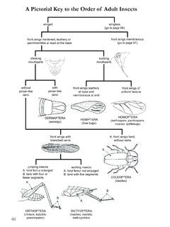
A Pictorial Key to the Order of Adult Insects
extension.entm.purdue.edufront wings hardened, leathery or parchmentlike at least at the base front wings membranous (go to page 61) chewing mouthparts sucking mouthparts without pincer-like cerci with pincer-like cerci front wings leathery at base and membranous at end front wings of uniform texture DERMAPTERA (earwigs) HEMIPTERA (true bugs) HOMOPTERA (leafhoppers ...

DEFENSE INTELLIGENCE BALLISTIC MISSILE ANALYSIS …
media.defense.govJan 11, 2021 · hardened structure, such as a bunker, to destroy its contents. A tandem penetrator can utilize an explosively formed projectile to create a pilot hole that a follow-through grenade can pass. These penetrators are likely effective against metallic structures such as hangars and carrier decks.-----

Valve model number description - Honeywell
products.ecc.emea.honeywell.com1 - 400 series stainless steel seat, hardened ductile iron disc, PEEK follower ring 2 - 316SS seat, 316SS disc, PEEK follower ring 4 - Oxy clean, trim 2 Body seals and bumper: - Buna o-rings/Buna bumper - Viton o-rings/Buna bumper - Viton o-rings/Viton bumper - Ethylene Propylene o-rings/Ethylene Propylene bumper - Omniflex o-rings/Buna bumper

GP5500 GP SERIES GP5500 - Generac Power Systems
www.generac.com• Hardened 1 1/4" steel tube cradle for added durability and strength. • Fold-down, locking handle for sturdy portability and compact storage. • Hour Meter tracks maintenance intervals. • Heavy-duty, never flat wheels for reliable portability. • Covered outlets provides added protection from the environment and rugged working conditions.

GP3300 GP SERIES GP3300 - Generac Power Systems
www.generac.com• Hardened steel tube cradle for added durability and strength. • old-down F handle for sturdy portability and compact storage. • Hour Meter tracks maintenance intervals. • Heavy-duty, never flat wheels for reliable portability. • 20A to 30A RV adapter makes your RV and your generator compatible. (1) 120/240V 20A L14-20R Twist Lock Outlet

Stormwater Best Management Practices: Concrete Washout
www3.epa.govhardened concrete that remains can be crushed (Fig. 6) and reused as a construction material. It makes an excellent aggregate for road base and can be used as fill at the construction site or delivered to a recycler. Concrete recyclers can be found at municipal solid waste disposal facilities, private recycling plants, or large construction sites.