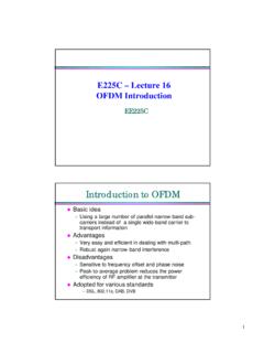
Introduction to OFDM
OFDM Introduction EE225C Introduction to OFDM lBasic idea » Using a large number of parallel narrow-band sub-carriers instead of a single wide-band carrier to transport information lAdvantages » Very easy and efficient in dealing with multi-path » Robust again narrow-band interference lDisadvantages » Sensitive to frequency offset and phase ...
Download Introduction to OFDM

Information
Domain:
Source:
Link to this page:
Documents from same domain

chapter2.fm Page 33 Monday, September 4, 2000 …
bwrcs.eecs.berkeley.eduIC packaging Future Trends in Integrated Circuit Technology 2.1 Introduction 2.2 Manufacturing CMOS Integrated Circuits 2.2.1 The Silicon Wafer 2.2.2 Photolithography 2.2.3 Some Recurring Process Steps ... cess that lies at the core of the semiconductor revolution. Yet, some insight in the steps ...

Designing a Divider - University of California, Berkeley
bwrcs.eecs.berkeley.eduDigital Integrated Circuits 2/e DIVIDE HARDWARE Version 1 ° 64-bit Divisor reg, 64-bit ALU, 64-bit Remainder reg, 32-bit Quotient reg Remainder Quotient Divisor …
CMOS Manufacturing Process
bwrcs.eecs.berkeley.eduDigital Integrated Circuits Manufacturing Process EE141 A Modern CMOS Process p-well n-well p+ p-epi SiO 2 AlCu poly n+ SiO 2 p+ gate-oxide Tungsten TiSi 2 Dual-Well Trench-Isolated CMOS Process
Lecture 9: Digital Signal Processors: Applications and ...
bwrcs.eecs.berkeley.eduProcessor Applications General Purpose - high performance ... Digital camera - TMS320C5000 ... DSP evolved from Analog Signal Processors, using analog hardware to transform phyical signals (classical electrical engineering) ASP to DSP because

DESIGNING COMBINATIONAL LOGIC GATES IN CMOS
bwrcs.eecs.berkeley.edu198 DESIGNING COMBINATIONAL LOGIC GATES IN CMOS Chapter 6 6.1Introduction The design considerations for a simple inverter circuit ere presented in the previousw chapter. In this chapter, the design of the inverter will be extended to address the synthesis

DESIGNING SEQUENTIAL LOGIC CIRCUITS
bwrcs.eecs.berkeley.edu272 DESIGNING SEQUENTIAL LOGIC CIRCUITS Chapter 7 7.1 Introduction Combinational logic circuits that were described earlier have the property that the output

Lecture11-MOS Cap Delay
bwrcs.eecs.berkeley.eduEE141 25 EECS141 Lecture #11 25 The Miller Effect V in M1 C gd1 V out ∆V As V in increases, V out drops – Once get into the transition region, gain from V in to V out > 1 So, C gd experiences voltage swing larger than V

Chapter 4 Calculating the Logical Effort of Gates
bwrcs.eecs.berkeley.edu4.3 Calculating logical effort Definition 4.2 provides a convenient method for calculating the logical effort of a logic gate. We have but to design a gate that has the same current drive character-istics as a reference inverter, calculate the input capacitances of each signal, and apply Equation 4.1 to obtain the logical effort.

DESIGNING COMBINATIONAL LOGIC GATES IN CMOS
bwrcs.eecs.berkeley.eduof arbitrary digital gates such as NOR, NAND and XOR. The focus will be on combina-tional logic (or non-regenerative) circuits that have the property that at any point in time, the output of the circuit is related to its current input signals by some Boolean expression (assuming that the transients through the logic gates have settled).

SEMICONDUCTOR MEMORIES
bwrcs.eecs.berkeley.eduThe read-out of the 1T DRAM cell is destructive; read and refresh operations are necessary for correct operation. Unlike 3T cell, 1T cell requires presence of an extra capacitance that must be explicitly included in the design. When writing a “1” into a DRAM cell, a threshold voltage is lost.
Related documents

MIMO-OFDM
www.ee.iitm.ac.in4.2 Basic Principle of OFDM 121 4.2.1 OFDM Modulation and Demodulation 121 4.2.2 OFDM Guard Interval 126 4.2.3 OFDM Guard Band 132 4.2.4 BER of OFDM Scheme 136 4.2.5 Water-Filling Algorithm for Frequency-Domain Link Adaptation 139 4.3 Coded OFDM 142 4.4 OFDMA: Multiple Access Extensions of OFDM 143

Aruba 500 Series Wireless Access Points Data Sheet
content.etilize.com• 802.11a/g/n/ac: Orthogonal frequency-division multiplexing (OFDM) • 802.11ax: Orthogonal frequency-division multiple access (OFDMA) with up to 8 resource units Supported modulation types: • 802.11b: BPSK, QPSK, CCK

IEEE 802.11 Standards: Wi-Fi 6 and beyond
futurenetworks.ieee.orgSlide 11 • Next Generation Positioning P802.11az project is the evolutionary roadmap of accurate 802.11 location (FTM) appearing first in previous revisions of the 802.11 standard: • Accurate indoor Navigation (sub 1m and into the <0.1m domain). • Secured (authenticated and private) positioning –open my car with my smartphone,

6G: Envisioning the Key Technologies, Applications and ...
thesai.orgorthogonal frequency division multiplexing (OFDM) and multiple-input multiple-output (MIMO) and user-sensitive goal of1000 times price reduction. Initial 3G users are limited to business community to access company resources and emails, while further enhancement occurs only after the deployment of 4G networks.

WiFi Sensing with Channel State Information: A Survey
www.cs.wm.eduFor a WiFi system with MIMO-OFDM, CSI is a 3D matrix of ... 11, 34, 53, 54, 82, 96, 97, 118, 124, 133, 139]. CSI phase shifts in the spatial and frequency domains, i.e., transmit/receive antennas and carrier frequencies, are related to signal transmission delay and direction, which can be used for human localization

User Manual - EnGenius Tech
www.engeniustech.com11 Windows XP/Windows 7/Windows 8/Windows 10 In orderto use the AccessPoint,you must firstconfigure the TCP/IPv4 connection of your Windows OS computer system. 1a. Click the Start button and open the Control Panel 1b. Move your mouse to the lower right hot corner to display the Charms Bar and select the Control Panel in Windows 8 OS. 1c.

esp-wroom-02u esp-wroom-02d datasheet en
www.espressif.comOFDM, 6 Mbps - 37 - dB OFDM, 54 Mbps - 21 - dB HT20, MCS0 - 37 - dB HT20, MCS7 - 20 - dB Description Min Typ Max Unit! Note: For the module that uses an IPEX antenna, the output impedance is 50 Ω. Table 4-3. Power Consumption –!

RF Power LDMOS Transistor - NXP
www.nxp.com11.2 W W/ C Table 2. Thermal Characteristics Characteristic Symbol Value (2,3) Unit Thermal Resistance, Junction to Case CW: Case Temperature 99 C, 1800 W CW, 65 Vdc, IDQ(A+B) = 150 mA, 98 MHz R JC 0.09 C/W Thermal Impedance, Junction to Case Pulse: Case Temperature 65 C, 1800 W Peak, 100 sec Pulse Width, 20% Duty Cycle,