
Lecture11-MOS Cap Delay
1.7 1.9 2.1 2.3 2.5 t/τ V OUT NMOS RC EE141 33 EECS141 Lecture #11 33 Finding Req () (), 2 1 ppRC + DD eq DD DSAT t=t CV RC λVI = ln 2 ()( ) 2 1 = + DD eq DDDSAT V R ln 2 λVI • Match the delay of the RC model with the actual delay: • Often just: () 1 ≈ ⋅ DD eq DSAT V R 2ln2I • Note that the book uses a different method and gets 0 ...
Download Lecture11-MOS Cap Delay

Information
Domain:
Source:
Link to this page:
Documents from same domain

chapter2.fm Page 33 Monday, September 4, 2000 …
bwrcs.eecs.berkeley.eduIC packaging Future Trends in Integrated Circuit Technology 2.1 Introduction 2.2 Manufacturing CMOS Integrated Circuits 2.2.1 The Silicon Wafer 2.2.2 Photolithography 2.2.3 Some Recurring Process Steps ... cess that lies at the core of the semiconductor revolution. Yet, some insight in the steps ...

Designing a Divider - University of California, Berkeley
bwrcs.eecs.berkeley.eduDigital Integrated Circuits 2/e DIVIDE HARDWARE Version 1 ° 64-bit Divisor reg, 64-bit ALU, 64-bit Remainder reg, 32-bit Quotient reg Remainder Quotient Divisor …
CMOS Manufacturing Process
bwrcs.eecs.berkeley.eduDigital Integrated Circuits Manufacturing Process EE141 A Modern CMOS Process p-well n-well p+ p-epi SiO 2 AlCu poly n+ SiO 2 p+ gate-oxide Tungsten TiSi 2 Dual-Well Trench-Isolated CMOS Process
Lecture 9: Digital Signal Processors: Applications and ...
bwrcs.eecs.berkeley.eduProcessor Applications General Purpose - high performance ... Digital camera - TMS320C5000 ... DSP evolved from Analog Signal Processors, using analog hardware to transform phyical signals (classical electrical engineering) ASP to DSP because

DESIGNING COMBINATIONAL LOGIC GATES IN CMOS
bwrcs.eecs.berkeley.edu198 DESIGNING COMBINATIONAL LOGIC GATES IN CMOS Chapter 6 6.1Introduction The design considerations for a simple inverter circuit ere presented in the previousw chapter. In this chapter, the design of the inverter will be extended to address the synthesis

DESIGNING SEQUENTIAL LOGIC CIRCUITS
bwrcs.eecs.berkeley.edu272 DESIGNING SEQUENTIAL LOGIC CIRCUITS Chapter 7 7.1 Introduction Combinational logic circuits that were described earlier have the property that the output
Chapter 4 Calculating the Logical Effort of Gates
bwrcs.eecs.berkeley.edu4.3 Calculating logical effort Definition 4.2 provides a convenient method for calculating the logical effort of a logic gate. We have but to design a gate that has the same current drive character-istics as a reference inverter, calculate the input capacitances of each signal, and apply Equation 4.1 to obtain the logical effort.

DESIGNING COMBINATIONAL LOGIC GATES IN CMOS
bwrcs.eecs.berkeley.eduof arbitrary digital gates such as NOR, NAND and XOR. The focus will be on combina-tional logic (or non-regenerative) circuits that have the property that at any point in time, the output of the circuit is related to its current input signals by some Boolean expression (assuming that the transients through the logic gates have settled).
Introduction to OFDM
bwrcs.eecs.berkeley.eduOFDM Introduction EE225C Introduction to OFDM lBasic idea ... – Selective Fading – Very short pulses – ISI iscompartively long – EQs are then very long – Poor spectral efficiency because of band guards Drawbacks ... 2 4 6 8 10 12 14 16-60-55-50-45-40-35-30-25-20-15-10

SEMICONDUCTOR MEMORIES
bwrcs.eecs.berkeley.eduThe read-out of the 1T DRAM cell is destructive; read and refresh operations are necessary for correct operation. Unlike 3T cell, 1T cell requires presence of an extra capacitance that must be explicitly included in the design. When writing a “1” into a DRAM cell, a threshold voltage is lost.
Related documents

BIOS-enabled security features in HP business notebooks
h10032.www1.hp.com1. Boot the system, and press f10 to enter the BIOS setup. 2. Select Setup BIOS Administrator Password from the Security menu. 3. Follow the prompts to create and confirm the new administrator password. The BIOS administrator sets up the BIOS user password as follows: 1. Boot the system, and then press f10 to enter the BIOS setup. 2.

SEVERITY LEVELS SPECIFIERS Early Remission = 3 months to 1 ...
cchealth.orgF10.21 303.90 Alcohol Use Disorder Severe, In early or sustained remission F10.129 303.00 Alcohol Intoxication with Use Disorder, Mild F10.229 303.00 Alcohol Intoxication with Use Disorder, Moderate or Severe F10.929 303.00 Alcohol Intoxication without Use Disorder F10.239 291.81 Alcohol Withdrawal without Perceptual Disturbances

B CITY CAMPUS 5 6 7 89 1011 12 13 14 15 E
cdn.auckland.ac.nzDance Studies 113, 820 F10, D9 DELNA 315 G9 Digital Services 435 I8 Disability Services 105 F9 Drama Studio 206 G10 Economics, Dept of 260 G,H10 Education (Liberal Arts Programme) 201E G10 Elam School of Fine Arts 113, 431-433 F10, I8, I9 Electrical & Computer Engineering, Dept of 301, 303, 401 H9, G9 Engineering, Faculty Office 401 H9

C Programming in Atmel Studio 7 - Nicer Land
nicerland.com7. The I/O tab appears on the right hand side which shows the peripherals of the microcontroller, including the I/O ports. Select PORTB. The values of the related registers (PINB, DDRB, and PORTB) will be shown below. 8. Press F10 (Step Over) a few times and see the PORTB register changes in the I/O. Using Breakpoints

DSM-5 UPDATE - Psychiatry
psychiatryonline.orgTrauma- and Stressor-Related Disorders .....1 7 . Acute Stress Disorder: Criterion A [October 2018] Adjustment Disorder: Addition of Acute and Persistent Specifiers [March 2014] ... F10.11 . Alcohol Use Disorder, Moderate F10.20 F10.20 Alcohol Use Disorder, Moderate, In early or sustained remission F10.20 .

Effective 9/7/2021 Rock Island District Line
schedules.metrarail.comEffective 9/7/2021 Rock Island District Line 400 600 402 602 404 604 300 700 606 302 702 608 304 704 610 412 612 414 614 416 618 418 620 420 622 422 624 424 626 426 628 428 630 430 632 432 512 514 516 518
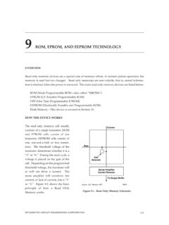
ROM, EPROM, and EEPROM Technology
web.eecs.umich.edupreviously, or, more commonly, in the NOR configuration shown in Figure 9-7. EPROMs were created in the 1970s and have long been the cornerstone of the non-volatile memory market. But the development of flash memory devices (see Section 10) will lead to a loss of EPROM marketshare. EPROM uses a mature technology and design and is on the decline ...